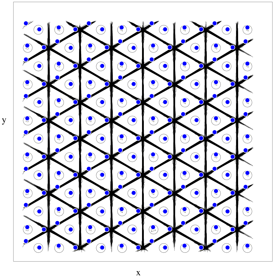
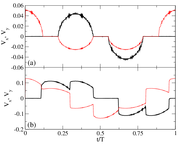
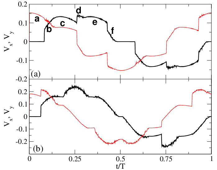
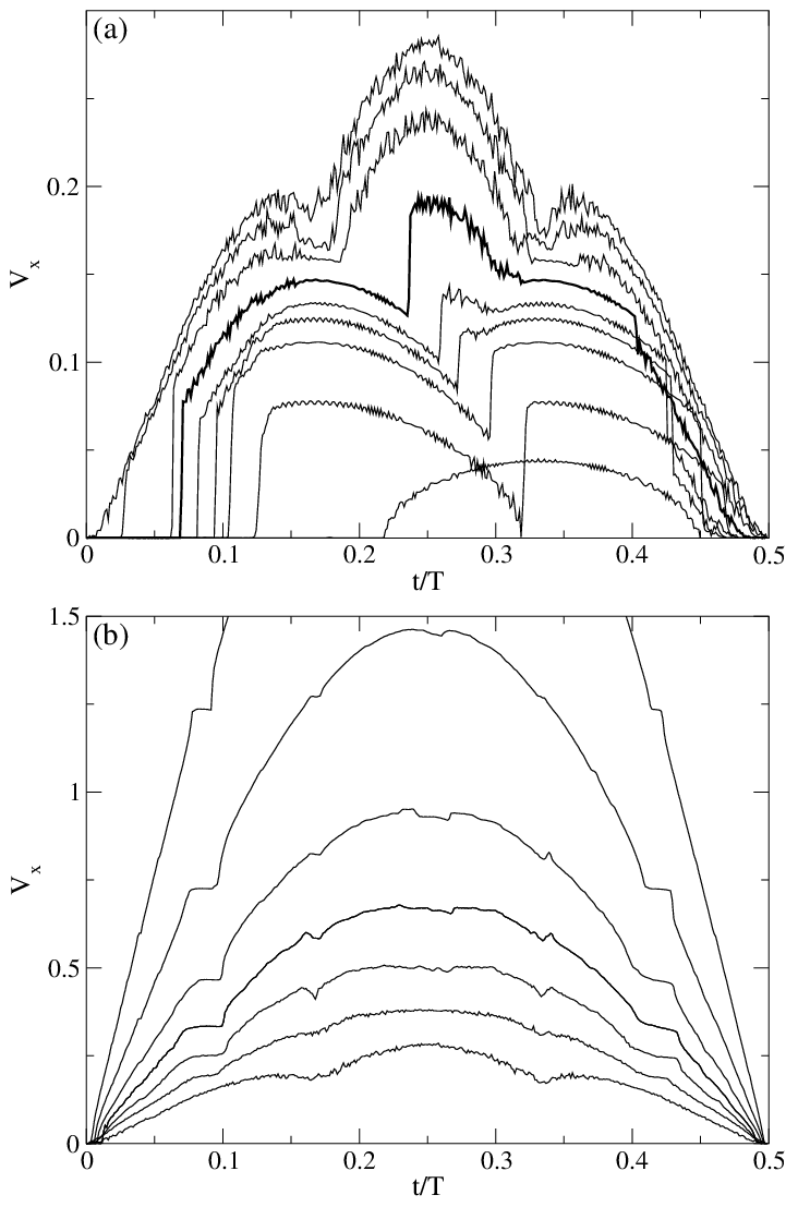
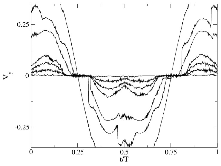
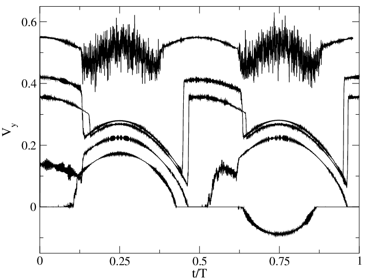
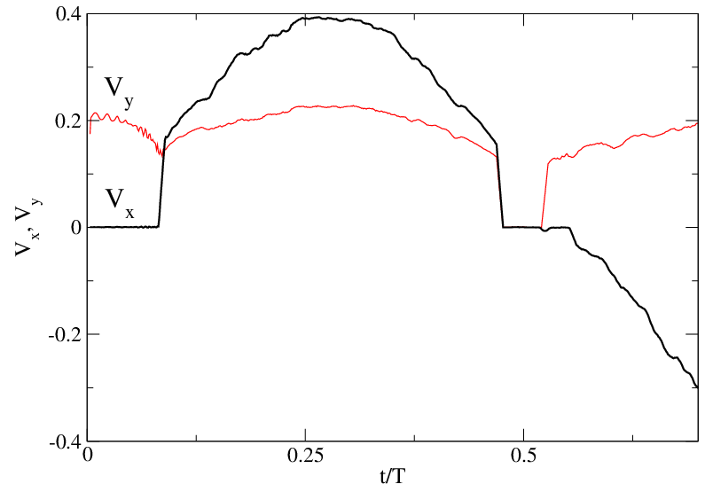
Physical Review B 81, 024510 (2010)

Switching and Jamming Transistor Effect for Vortex Matter in Honeycomb Pinning Arrays with ac Drives

C. Reichhardt and C.J. Olson Reichhardt

Theoretical Division, Los Alamos National Laboratory, Los Alamos, New Mexico 87545, USA

(Received 10 June 2009; published 12 January 2010)

We show that a remarkable variety of dynamical phenomena, including switching, polarization, symmetry locking, and dynamically induced pinning, can occur for vortices in type-II superconductors in the presence of a honeycomb pinning array and an ac or combined ac and dc drive. These effects occur at the second matching field where there are two vortices per pinning site, and arise due to the formation of vortex dimer states in the interstitial regions of the honeycomb array. The orientation of the pinned and moving vortex dimers can be controlled externally by the application of a drive. We term this a polarization effect and demonstrate that it can lock or unlock the vortex motion into different symmetry directions of the underlying pinning lattice. If the moving vortices are locked into one direction, the motion can be switched into a different direction by applying an additional bias drive, producing sharp jumps in the transverse and longitudinal velocities. Further, the dc vortex motion in one direction can be controlled directly by application of a force in the perpendicular direction. When the moving dimers reorient, we find a remarkable dynamical pinning effect in which the dimers jam when they become perpendicular to the easy flow direction of the pinning lattice. Since application of an external field can be used to switch off the vortex flow, we term this a jamming transistor effect. These effects do not occur in triangular pinning arrays due to the lack of the n-merization of the vortices in this case. The switching and dynamical pinning effects demonstrated here may be useful for the creation of new types of fluxtronic devices.
I. INTRODUCTION
II. SIMULATION
III. EXTERNAL CONTROL OF THE VORTEX DIMER ORIENTATION
A. High ac Amplitude and Order-Disorder Transitions
B. Vortex Velocity Evolution with ac Amplitude
C. Commensurability Effects Near the B/Bϕ = 2.0 State
D. ac Effects on the Vortex Trimer State at B/Bϕ = 2.5
IV. FIXED DC DRIVE IN THE Y-DIRECTION WITH AN AC DRIVE IN THE X-DIRECTION
A. Jamming Transistor Effect
B. Varied ac Amplitude and Fixed dc Amplitude
C. Constant ac Amplitude and Varied dc Amplitude
D. Commensurability Effects
V. MODIFIED VORTEX INTERACTIONS FOR THIN FILM SUPERCONDUCTORS
VI. DISCUSSION
VII. SUMMARY
References

I.  INTRODUCTION

The dynamics of vortices in type-II superconductors has attracted enormous interest since they can provide insight into both the nonequilibrium phases of driven particles moving over a quenched landscape as well as properties of vortex dynamics that can be useful for creating new types of fluxtronic devices. In terms of basic science, driven vortices are an ideal system in which to study different types of nonequilibrium phase transitions [1,2,3,4,5,6,7]. It appears that nonequilibrium systems can undergo transitions between specific types of driven phases similar to the transitions among equilibrium phases that occur as a parameter is tuned. Vortices driven over a randomly disordered substrate can pass through a pinned phase, a disordered or plastic flow phase with large fluctuations [1,5,6], and different types of moving phases which may be partially ordered in one direction to form a moving smectic [4,5,7] or have moving crystal symmetry [3,4,7]. Other types of phases are also possible within the plastic flow regime, including chaotic [8], reversible, and irreversible flows [9]. For driven vortices in samples with periodic pinning arrays, an exceptionally rich variety of distinct dynamical behaviors appear [10,11,12,13,14,15,16,17,18,19,20,21,22,23,24,25]. Periodic pinning arrays in superconductors can be created with nanoholes [26,27,28,29,30,31,32,33,34,35,36,37,38] or magnetic dots [39,40,41]. Typically, strong matching effects are observed in these samples as anomalies in the critical current or other transport measurements when the number of vortices equals an integer multiple or rational fraction of the number of pinning sites. At the matching field Bϕ, there are an equal number of vortices and pins. Above the first matching field, the additional vortices corresponding to the excess density BBϕ can be located in the interstitial regions between the occupied pinning sites already occupied by vortices [14,29,30,10,33,34] or multiple vortices can be trapped at each pinning site [29,30,34,35,36]. If interstitial vortices are present, they are more mobile than the pinned vortices under an applied drive and have a lower depinning threshold, so the interstitial vortices can move around the pinned vortices as observed in experiments [14,15] and simulations [10,13]. The interstitial vortex motion can be probed by adding an ac drive to a dc drive to produce Shapiro steps in the current-voltage curves [15]. The symmetry of the underlying pinning array can lock the vortex motion into particular directions when the vortices are driven at various angles with respect to the pinning lattice, as predicted in simulations [19] and demonstrated in experiment [20,21,22]. In addition to the superconducting system, vortices interacting with periodic substrates can also be realized in Bose-Einstein condensates with a periodic optical trap array [42,43,44], opening a new avenue for the study of vortex matter on dynamical substrates.
Studies of vortices interacting with periodic pinning arrays have primarily concentrated on triangular or square arrays; however, other types of pinning geometries such as honeycomb or kagomé arrays can also be realized in experiment [38,41]. A honeycomb pinning array is constructed from a triangular array by removing 1/3 of the pinning sites, while a kagomé array is generated by removing 1/4 of the pinning sites. Experiments have shown that honeycomb and kagomé pinning arrays exhibit anomalies in the critical currents at non-matching fields as well as at matching fields [38,41]. In honeycomb pinning arrays, non-matching anomalies occur at fields B/Bϕ=n + 1/2, where n is an integer. This suggests that a portion of the vortices are trapped in the large interstitial regions in such a way as to match the original undiluted triangular pinning array. Simulations also reveal matching effects at integer and half integer matching fields up to B/Bϕ=5 for honeycomb arrays, and indicate that this type of matching can occur when multiple interstitial vortices are trapped at the large interstitial sites in the honeycomb array and form either ordered vortex molecular crystals or vortex plastic crystals [45]. In vortex molecular crystals, the vortices in the large interstitial site behave as n-mer objects that have a director field which can be oriented in different directions with respect to the pinning lattice. The n-mers can have long range order and may experience ferromagnetic coupling that aligns the n-mers in a single direction, antiferromagnetic coupling that causes neighboring n-mers to orient perpendicularly to each other, or other types of coupling that produce ordered phases [45]. Vortex molecular crystals form at integer and half integer matching fields when B/Bϕ ≥ 2 for honeycomb pinning arrays and at integer multiples of B/Bϕ=1/3 for kagomé pinning arrays [45]. Vortex plastic crystals occur when the temperature is high enough to destroy the orientational order of the vortex n-mers. Experiments show that as the temperature increases, certain commensuration peaks disappear, which is consistent with the formation of plastic vortex crystals [38,45].
The vortex n-merization in honeycomb pinning arrays produces a novel dynamical symmetry breaking effect [46,47]. At B/Bϕ = 2, the vortices form dimers with a broken ground state symmetry. When a longitudinal drive is applied, there is a positive or negative transverse velocity response from the moving dimers depending on the direction of the original symmetry breaking. At incommensurate fields near B/Bϕ=2 where dimers are present, the ground state is not globally symmetry broken; however, under a longitudinal drive the moving dimers can dynamically organize into one of two possible flow states with a transverse response. When the longitudinal drive is held fixed at a constant value, the direction of the transverse flow can be switched with an externally applied dc transverse drive. Both the transverse and longitudinal velocities change abruptly when the flow direction switches. If the amplitude of the transverse drive is too weak, the system remains locked in the original transverse flow direction. When an ac transverse drive is applied in addition to a fixed dc longitudinal drive, the transverse portion of the vortex flow oscillates, resulting in an amplification of the transverse response in certain regimes. In these regimes, an increase of the transverse ac force can cause the longitudinal vortex velocity to decrease. The pronounced switching and amplification behaviors of the vortex dimers may be useful for producing transistorlike devices [48,49].
In this work, we study the vortex dimer response in a sample with a honeycomb pinning lattice subjected to ac or combined ac and dc drives. We find switching and jamming phenomena and a rich variety of dynamical behaviors. Many of our results should be relevant for systems other than vortices on periodic pinning arrays. Simulations, theory, and experiments have shown that colloidal particles interacting with a periodic substrate can exhibit an n-merization effect at fillings where there is more than one colloid per substrate minimum [50,51,52,53]. These states have been termed colloidal molecular crystals and have many of the same properties as the vortex molecular crystals [45,46,47]. Our results may also apply to other systems such as molecular dimers driven over periodic substrates, friction systems [54], or charged balls on periodic substrates [55]. The symmetry locking effect predicted for vortices moving over periodic arrays [19] has been observed in experiments with colloids moving over periodic arrays [56]. We thus expect that the results described in this work should be generic for colloids on honeycomb arrays.

II.  SIMULATION

We simulate a two-dimensional system of size L ×L with periodic boundary conditions in the x and y directions containing Nv vortices at a density nv=Nv/L2. The vortex density nv is proportional to the magnetic field B=Bz. Vortices can move under the influence of the Lorentz force from an applied current J or due to interactions with the other vortices. In a type-II superconductor the vortex core is not superconducting, so the vortex motion is overdamped due to dissipation of energy by the core. The motion of vortex i at position Ri is governed by the following equation of motion:

η dRi

dt
= Fivv + Fpi + Fdc + Fac + FTi .
(1)
Here the damping constant η = ϕ02d/2πξ2ρN, where d is the sample thickness, ϕ0=h/2e is the flux quantum, ξ is the superconducting coherence length, and ρN is the normal state resistivity of the material. The repulsive vortex-vortex interaction force is
Fivv = Nv

ji 
f0K1
Rij

λ

^
R
 

ij 
,
(2)
where K1 is the modified Bessel function, λ is the London penetration depth, f002/(2πμ0λ3), the distance between vortices i and j is Rij = |RiRj|, and Rij = (RiRj)/Rij. We measure lengths in units of λ and take L=24λ so that the system size is 24λ×24λ. Since the vortex-vortex interaction force falls off rapidly with Rij, we impose a long range cutoff at 6λ. For very short Rij a cutoff is placed at 0.1λ to avoid a divergence in the force.
The force from the vortex-pinning site interactions is Fpi. We place Np pinning sites, with a pinning density of np = Np/L2, in a honeycomb array formed by removing every third pinning site from a triangular array. The pinning sites have a maximum force of Fp=0.85 and a fixed radius of rp=0.35λ, which is small enough that only one vortex is trapped per pinning site. Each pinning potential is modeled as an attractive parabolic well, giving a force
Fpi = Np

k=1 
FpRik(p)f0

rp
Θ
rpRik(p)

λ

^
R
 
(p)
ik 
.
(3)
Here Θ is the Heaviside step function, Rk(p) is the location of pinning site k, R(p)ik = |RiR(p)k|, and R(p)ik = (RiR(p)k)/R(p)ik. The matching field Bϕ is defined as the field with Nv=Np where there is one vortex per pinning site. We fix Bϕ=0.3125ϕ02. In Fig. 1 we illustrate the pinning site positions and vortex locations for a honeycomb pinning array at B/Bϕ = 2.0.
Fig1.png
Figure 1: Vortex positions (filled dots) and pinning site locations (open circles) for a honeycomb pinning array with B/Bϕ = 2.0. Here the interstitial vortices form a dimer state. A circular ac drive is applied with A = 0.075 and T=3.14×10⁶ simulation time steps. (a) In the initial state at t=0 the dimers are aligned along the y-direction at θ = π/2. (b) At t/T=0.25, the dimers are tilted to θ = 5π/6. (c) At t/T=0.54, the dimers are in the process of switching to a new symmetry direction. (d) At t/T=0.6, the dimers have switched to the orientation θ = 7π/6.
The thermal force FTi is modeled as random Langevin kicks with the correlations 〈FTi〉 = 0 and 〈FiT(t)FjT(t)〉 = 2ηkBT δ(ttij. We obtain the initial vortex configurations by simulated annealing. In this study we anneal by starting at fT=3.0 and spend 5000 simulation time steps at each temperature before reducing the temperature in increments of δfT=0.002. Slower annealing times do not change the final T = 0 vortex configurations.
Once the vortex configuration is initialized, we apply a uniform dc drive Fdc=Fdcy and ac drive Fac. Unless otherwise noted, the ac force has the form
Fac = Af0
sin(2πt/T)
^
x
 
+ cos(2πt/T)
^
y
 

,
(4)
with amplitude A and period T. We measure the average vortex velocity response Vx=Nv−1〈∑i=1Nvvi·x〉 and Vy=Nv−1〈∑i=1Nvvi·y〉, where vi is the velocity of vortex i. We note that the ability to apply currents in both x and y directions and measure the voltage response has been demonstrated experimentally [20,21,22].

III.  EXTERNAL CONTROL OF THE VORTEX DIMER ORIENTATION

We first consider a honeycomb pinning lattice at B/Bϕ = 2.0 with a circular ac drive and no dc drive. At this matching field, the interstitial vortices form dimer states in the large interstitial regions of the honeycomb pinning lattice, as shown in Fig. 1(a) and studied previously in Ref. [45]. The dimers have an effective ferromagnetic coupling and are all aligned in the same direction. In previous work we showed that in the absence of a drive, the ground state configuration of the dimers can be aligned in one of three directions [45]. Here we show that an external ac drive can couple to the dimers and change their orientation provided that the ac amplitude is small enough that the interstitial vortices do not depin.
In Fig. 1 we illustrate the time evolution of a system under an ac drive with A=0.075 and T=3.14×10⁶ simulation time steps. The dimers are initially aligned in the y-direction as shown in Fig. 1(a). We denote the direction of the dimer orientation as θ, measured on the unit circle. Here, the initial orientation is θ = π/2. The ac drive induces two types of dimer motion. The first is a rotation of the dimers in phase with the ac drive and the second is an abrupt switching where the dimers suddenly change their orientation to a new symmetry direction. We characterize these different types of motion by examining the vortex positions and trajectories as well as the time traces of Vx and Vy. Fig. 1(b) shows a snapshot of the dimer positions at t/T=0.25 when the dimers have tilted to align at θ = 5π/6. At t/T=0.54 the dimers are in the process of switching between θ = 5π/6 and θ = 7π/6, and align as shown in Fig. 1(c) to form an overall stripelike pattern that incorporates the pinned vortices. In Fig. 1(d) at t/T=0.6, the dimers have switched to an alignment of θ = 7π/6. The time sequence shows that the dimers rotate in phase with the circular ac drive.
In Fig. 2 we plot the vortex trajectories corresponding to the system shown in Fig. 1. The first two switches in the cycle (during a time interval of 0.6T) appear in Fig. 2(a), while Fig. 2(b) indicates that the dimers move in a closed triangular orbit during a complete cycle. A combination of smooth and switching dimer motion appears in Vx and Vy as a function of time in Fig. 3. The sinusoidal envelopes of the velocity traces are interlaced with spike features formed when the dimers abruptly switch to a new orientation. The first jump at t/T=0.2 occurs at the transition from the θ = π/2 orientation shown in Fig. 1(a) to the θ = 5π/6 orientation shown in Fig. 1(b). The lower vortex in each dimer shifts in the positive x direction with a smaller displacement in the negative y direction, while the other vortex in the dimer shifts in the negative y direction with a smaller displacement in the negative x direction. The sum of these motions gives a positive Vx pulse and a simultaneous negative Vy pulse in Fig. 3. In the next switching event at t/T=0.54, the upper vortex in each dimer shifts in the negative y direction while the other dimer vortex shifts in the positive y direction, reducing the net value of Vy. At the same time, both vortices in the dimer move in the negative x direction, enhancing the magnitude of Vx as shown in Fig. 3. This process repeats each period. The switching behavior occurs since the vortex dimers sit in a caging potential with a sixfold modulation created by the repulsive interactions with the six vortices located at the neighboring pinning sites. This modulation provides an energy barrier for the switching of the dimer from one orientation to another. The field-induced switching effect we observe is similar to liquid crystal behavior where the orientation of rod shaped molecules can be altered with external fields. Thus, we term the dimer switching a polarization effect, and note that it could be used to create numerous novel vortex devices. For example, the orientation of the dimers can be rotated in such way as to maximize the critical current in certain directions. Additionally, logic states could be assigned with different logic values corresponding to different dimer orientations.
Fig2.png
Figure 2: Vortex positions (filled dots), pinning site locations (open circles), and vortex trajectories (lines) for the same system in Fig. 1. (a) The trajectories during a time interval of 0.6T when two switching events occur. (b) The trajectories during a time interval of 1.1T showing the complete vortex orbits. The interstitial vortices follow the same orbits for all later times.
Fig3.png
Figure 3: The instantaneous vortex velocity vs time for the system in Fig. 1. (a) Vx. (b) Vy. The spikes correspond to the abrupt switching events where the dimers change orientation.
The pinned switching behavior shown in Fig. 3 only occurs under certain conditions. If the ac amplitude A is small, the dimers are unable to switch and remain locked in a single orientation. Conversely, if the ac amplitude is too large, the dimers escape from the interstitial caging potential and channel along one of six angles: θ = π/6, π/2, 5π/6, 7π/6, 3π/2, or 11π/6. In Fig. 4(a,b) we plot Vx and Vy versus time for the same system in Fig. 3 but with a smaller ac amplitude of A=0.03 which is too weak to induce switching. The velocity curves are smooth and merely follow the ac input drive as the vortices shift slightly in the interstitial sites. When the external drive is large enough, the dimers depin from the large interstitial regions and channel along one of the six easy-flow directions of the lattice, giving the velocity response shown in Fig. 4(c,d) for A=0.125. The channeling effect is very pronounced due to the significant barriers that the vortices must overcome in order to lock their motion into a new easy-flow direction. In fact, the locking is so strong that when the vortices switch to a different flow direction they skip over every other easy-flow direction, so that only three of the possible six symmetry flow directions are followed in a given realization. Which of the two sets of three flow directions that the system chooses depends on the initial conditions. In Fig. 4(c,d) at A=0.125, the dimers initially flow along θ = π/2, similar to the motion shown in Fig. 5(a). Figure 4(c,d) indicates that during the first portion of the drive cycle, −0.15 ≤ t/T < 0.15, Vy is finite and Vx is zero, as expected for motion that is locked in the y direction. For 0.15 ≤ t/T < 0.5, the x component of the ac drive becomes strong enough to reorient the dimers so that they channel along a different symmetry direction. The vortices lock to θ = 11π/6 and have the same type of motion illustrated in Fig. 5(e). During 0.5 ≤ t/T < 0.85, the vortex motion switches and flows along θ = 7π/6. Finally the vortex motion returns to θ = π/2. In this cycle, the vortices never flow along θ = π/6, 3π/2, or 5π/6. By changing the initial conditions slightly, we can obtain vortex motion along those three angles only (and not along π/2, 11π/6, or 7π/6) with a fifty percent probability. For A=0.125, there are small windows of pinned phases between the sliding locked phases. In Fig. 6 we plot the vortex trajectories during an entire drive period showing the triangular pattern formed as the vortices flow along three different directions.
Fig4.png
Figure 4: (a) Vx and (b) Vy versus time for the same system in Fig. 1 with A = 0.03 where the dimers do not switch. (c) Vx and (d) Vy for the same system with A = 0.125 where the ac amplitude is high enough to induce a sliding of the dimers. In each driving period, the dimers initially slide along θ = π/2 in the positive y-direction, become pinned, and then slide along θ = 11π/6 and θ = 7π/6 in turn.
Fig5.png
Figure 5: Vortex positions (filled dots), pinning site locations (open circles), and vortex trajectories (lines) for the system in Fig. 1 at A=0.35 during half of a drive cycle. The points from which the images are taken are marked with bold letters in Fig. 8(a). (a) The dimers initially move in the y-direction, θ = π/2. (b) Transition to the disordered flow state in which a portion of the pinned vortices depin. (c) The dimers lock to θ = π/6. (d) Transition to another disordered flow state where a portion of the pinned vortices depin; the average velocity is in the x direction. (e) The dimers lock to θ = 11π/6. (f) Transition to a disordered flow state in which a portion of the pinned vortices depin. The remainder of the drive cycle has the same appearance as (a-f) but with the motion of the vortices reversed to follow θ = 3π/2, 7π/6, and 5π/6.
Fig6.png
Figure 6: Vortex positions (filled dots), pinning site locations (open circles), and vortex trajectories (lines) for the system in Fig. 4(c,d) at A = 0.125 during a complete drive cycle. The dimers slide along three different angles so the trajectories form a triangular pattern.
For ac amplitudes 0.11 < A ≤ 0.2, Fig. 7(a) shows that only three of the six possible flow directions appear and that Vx and Vy simultaneously drop to zero between the sliding regimes in each period, indicating the existence of a temporary pinned phase. For A > 0.2 the system passes directly from one siding state to another without pinning, as indicated in Fig. 7(b), and flow occurs in all six possible directions. Figure 7(b) shows that at A=0.3, Vx and Vy have discontinuities when the system switches from one flow direction to another, but that Vx and Vy are never simultaneously zero. Within a given flowing locked phase, Vx and Vy are not fixed but can show considerable variations.
Fig7.png
Figure 7: Vx (heavy line) and Vy (light line) versus time for the system in Fig. 1. (a) At A = 0.16 there are three pinned phases between the three sliding phases in each period. (b) At A = 0.3, the dimers are always sliding along the different symmetry directions and there are no pinned phases.
For 0.2 < A < 0.335, only the interstitial vortices are moving, while for A ≥ 0.335 a portion of the vortices located at the pinning sites become mobile during certain parts of the ac drive cycle. This produces additional disordered flow phases between the flowing locked phases. We plot Vx and Vy during one drive cycle at A=0.35 in Fig. 8(a) and show the corresponding vortex trajectories in Fig. 5. At the beginning of the drive cycle, the dimers are locked to flow along θ = π/2, as shown in Fig. 5(a). The system does not jump directly into an ordered channel flow of dimers along θ = π/6, but instead first passes through an intermediate flow state near point b in Fig. 8(a). The vortex trajectories are disordered, as shown in Fig. 5(b). Within this regime a portion of the vortices at the pinning sites depin due to the combination of the vortex-vortex interaction forces and the applied drive. The result is a random flow which appears as enhanced fluctuations in Vx and Vy. From the random phase, the system reorders into a locked flowing state along θ = π/6 illustrated in Fig. 5(c), where all the pinning sites are again occupied and the dimers move in an ordered fashion. The system then enters another disordered flow regime shown in Fig. 5(d). The transition into this disordered phase produces a jump in Vx. As the ac drive period progresses, the vortices lock into another flowing state along θ = 11π/6 illustrated in Fig. 5(e), followed by the disordered flow phase shown in Fig. 5(f). During the second half of the drive cycle, a similar series of ordered and disordered phases occur as the vortices successively lock into θ = 3π/2, θ = 7π/6, and θ = 5π/6, before finally returning back to the starting point of locked flow along θ = π/2. In all cases, the random flow phases are associated with increased fluctuations of Vx and Vy. The vortex velocity distributions are broadened in the random flow phase, whereas in the ordered flow phases the velocities are synchronized.
Fig8.png
Figure 8: Vx (heavy lines) and Vy (light lines) versus time for the same system in Fig. 1. (a) At A = 0.35, a portion of the vortices at the pinning sites start to depin and generate random phases between the locked sliding phases. The labels a, b, c, d, e, and f correspond to the portions of the period illustrated in Fig. 5. The disordered flow phases appear at b, d, and f during the transitions between different locked sliding states. (b) At A = 0.405, the random flow phases are broader.
In Fig. 8(b) we plot Vx and Vy versus time for A = 0.405 where only a small window of each locked sliding phase occurs between the random flow regimes. For A > 0.42, the locked sliding phases vanish and the flow is disordered throughout the ac drive cycle, although some slight channeling persists within the random flow phase.
We summarize the results for 0 < A < 0.45 in a dynamic phase diagram in Fig. 9, where we plot the phases for A versus time during half an ac drive period. For A < 0.05 we find a pinned locked (PL) phase in which all the vortices remain pinned and the dimers do not show any switching behavior. The dashed line at A=0.05 separates the PL from the pinned switching (PS) regime where the dimers remain pinned but change orientation. For 0.11 < A < 0.16 the PS phase is lost over much of the drive cycle and is replaced by a series of sliding states along every other symmetry angle. Here, the vortices follow θ = π/2 and θ = 11π/6 in this half of the drive cycle, separated by the remnants of the PS phase. The PS regime disappears completely for A ≥ 0.16 and for 0.16 ≤ A < 0.3, the vortices lock into each symmetry angle in turn, passing from θ = π/2 to θ = π/6 to θ = 11π/6, and so forth. For 0.325 ≤ A < 0.435, the sliding phases are separated by intrusions of the random flow (R) phase which increase in extent until the sliding states are completely lost for A ≥ 0.435.
Fig9.png
Figure 9: The dynamic phase diagram for the system in Fig. 1 showing ac amplitude A vs time. For low A the dimers are in the pinned locked (PL) state. For 0.05 < A ≤ 0.11 the dimers are in the pinned switching (PS) state where they remain pinned but switch between different orientations as shown in Fig. 2 and Fig. 3. The dashed line separates the PL and PS phases. For 0.11 < A < 0.16, the vortices pass through a series of sliding phases along θ = π/2, θ = π/6, and θ = 11π/6. The sliding phases are separated by pinned phases for 0.11 < A < 0.16 and by random flow (R) phases for 0.325 < A < 0.435.

A.  High ac Amplitude and Order-Disorder Transitions

The vortices depin and flow in a random phase when the ac amplitude is large enough to overcome the pinning force. For even higher ac drive amplitudes, we find that the system enters a new dynamical regime. The vortex flow changes from the channeling of interstitial vortices between occupied pinning sites to a regime where all the vortices take part in the motion and a portion of the vortices move in locked channels that pass through the pinning sites. For ac amplitudes just above A=0.435 where the dimer channeling is lost, the system is disordered and the vortices undergo plastic flow in which some vortices are temporarily trapped at the pinning sites. The features in the velocity versus time curves are washed out and we find only a weak channeling of the vortex motion. In this regime, the vortex lattice is heavily defected. As the ac amplitude is further increased, the effectiveness of the pinning diminishes and the vortices begin to partially reorder along certain symmetry directions of the pinning lattice.
To quantify the reordering we use a Voronoi construction to measure the fraction of six-fold coordinated vortices P6=Nv−1i=1Nvδ(zi−6), where zi is the coordination number of vortex i. For a perfectly triangular vortex lattice, P6=1. In Fig. 10(a) we plot Vx and Vy vs time for A = 0.43, where the vortices are in the random flow (R) regime. Small features in Vx and Vy indicate the persistence of partial channeling even in the random flow phase. Figure 10(b) shows the corresponding measurement of P6, which has an average value of P6 ≈ 0.5 due to the highly defective nature of the vortex lattice in the random flow phase. At A=0.5, Fig. 10(c) indicates that the channeling features disappear and are replaced by new steplike features in Vx and Vy. Figure 10(d) shows that the steps are correlated with six maxima in P6, indicating that the vortices are partially ordered along the steps and that a different type of channeling effect is occurring. The overall vortex lattice remains disordered throughout the drive cycle; however, when the drive falls on a step, P6 ≈ 0.68, while between the steps, P6 ≈ 0.5.
Fig10.png
Figure 10: (a) Vx (dark line) and Vy (light line) versus time for the system in Fig. 9 at A=0.43, where the flow is disordered. Although the system is in the random phase, there is still some mild channeling of the vortices which appears as modulations of Vx and Vy. (b) The corresponding fraction of six-fold coordinated vortices P6 vs time. For a completely triangular lattice P6 = 1.0. Here P6 ≈ 0.5, indicating that the vortex lattice is disordered throughout the whole driving cycle. (c) Vx (dark line) and Vy (light line) versus time for the system in Fig. 9 at A = 0.5. The channeling effects are completely destroyed; however, new steplike features are beginning to appear. (d) The corresponding P6 vs time shows enhancements that are correlated with the steplike features in Vx and Vy, indicating that the vortices are gaining some partial ordering on the steps.
At A=0.75, shown in Fig. 11(a), the steps in Vx and Vy are much denser and are associated with a series of peaks and dips in P6, shown in Fig. 11(b). Between the steps, P6 ≈ 1, indicating a triangular vortex lattice, while on the steps, the vortices are less ordered and P6 ≈ 0.68. The changes in P6 indicate that the vortices undergo a series of order-disorder transitions during the ac drive cycle. The average minimum amount of vortex order present at A = 0.75 is larger than average maximum vortex order at A=0.5, as indicated by comparing P6 in Fig. 11(b) and Fig. 10(d). In Fig. 12(a) we show a blowup of Vx and Vy for 0.05 < t/T < 0.2 from Fig. 11(a) to highlight the order-disorder transition that occurs when the vortices enter and exit a single velocity step. We plot the corresponding P6 values in Fig. 12(b). Within the nonstep intervals, where Vx and Vy are smoothly increasing or decreasing, P6 ≈ 1, indicating that the vortices are mostly sixfold coordinated. The dashed lines in Fig. 12 outline the step located at 0.072 < t/T < 0.102. A dip in P6 occurs as the system both enters and exits this step, indicating enhanced disorder in the vortex lattice. On the velocity step, P6 increases to P6 ≈ 0.85 but the vortex lattice structure is not completely ordered. Outside of the step, the vortices regain a nearly triangular ordering until reaching the next velocity step at t/T ≈ 0.15. In Fig. 13 we plot the vortex trajectories for the system in Fig. 12 before, during, and after the step, where the step onset tstep/T=0.072. Below the step, Fig. 13(a) shows that the vortex trajectories are disordered, while on the step Fig. 13(b) shows more ordered vortex motion with a partial locking to θ = π/3. The vortices channel along the pinning sites rather than between them. Above the step, the vortex motion is again disordered, as illustrated in Fig. 13(c).
Fig11.png
Figure 11: (a) Vx (dark line) and Vy (light line) vs time for the same system in Fig. 10 with a higher ac amplitude of A = 0.75. (b) The corresponding P6 vs time shows a series of order to disorder transitions.
Fig12.png
Figure 12: A blowup of the region 0.05 < t/T < 0.2 from Fig. 11 with A=0.75 highlighting the order to disorder transitions across a step. (a) Vx (dark line) and Vy (light line) versus time. (b) The corresponding P6 vs time. The dashed lines highlight the transitions into and out of the step; the vortex positions are disordered at the transitions and more ordered on the step.
Fig13.png
Figure 13: Vortex positions (filled dots), pinning site locations (open circles), and vortex trajectories (black lines) for the system in Fig. 12. (a) (tstept)/T=0.06, below the locking step. The vortices are initially not locked to a specific angle. (b) In the center of the step region, (ttstep)/T=0.014, the vortices channel along θ = π/3. (c) Above the locking step, (ttstep)/T=0.06, the vortex trajectories are disordered.
The other velocity steps in Fig. 11(a) also correspond to regimes where the vortices channel along the pinning sites at different angles. This type of channeling motion along pinning sites was studied previously for vortices in square pinning arrays at fields close to the matching field B/Bϕ = 1.0 [19]. In that system, a fixed dc drive Fxd was applied in the longitudinal direction and a transverse dc drive Fyd was gradually increased. A series of steps in the transverse velocity appeared, forming a devil's staircase structure. The velocity steps form when the vortex motion is locked to certain angles with respect to the symmetry axis of the pinning array. Specifically, for a square array steps form at drive ratios of Fyd/Fxd = m/n, where m and n are integers. For a triangular pinning array, velocity steps occur when Fyd/Fxd = √m/2n +1. For the honeycomb array, we expect a similar set of velocity steps to occur at the same drive ratio values as in the triangular array, but unlike the triangular array, the steps should be particularly pronounced when the drive angle is along θ = π/3, θ = π/2, θ = 2π/3, or the complements of these angles. In Ref. [19], a series of order-disorder transitions were observed that are similar to the order-disorder transitions we find in the honeycomb array.
In Fig. 14(a) we plot the Voronoi construction of a snapshot of the vortex configuration at (tstept)/T=0.06, below the step highlighted in Fig. 12. In the non-step regions, the vortex lattice is almost completely triangularly ordered and contains only a small number of zi=5 and zi=7 paired defects. In Fig. 14(b) at t=tstep, the vortex lattice becomes strongly disordered and there is a proliferation of zi=5 and zi=7 defects. In the center of the velocity step at (ttstep)/T=0.014, Fig. 14(c) shows that the density of defects drops compared to Fig. 14(b). The remaining zi=5 and zi=7 defects are aligned in the direction of the channeling motion, which can be seen from the trajectory plots in Fig. 13(b). The defect alignment indicates that on the steps, the vortex lattice has the characteristics of a moving smectic. Above the step, as shown in Fig. 14(d) at (ttstep)/T=0.06, the vortices reorder into a nearly triangular lattice. A similar set of vortex lattice structures appear for each step and the topological defects align in the channeling direction on the steps. At the transitions on and off of each step, the vortex lattice disorders when a portion of the vortices move in a channeling direction while another portion of the vortices move in the driving direction. This combination of vortex motion disorders the lattice.
We note that in general we do not observe complete locking, and even on a step, not all the vortices align with the drive as shown in Fig. 13(b). Much stronger velocity steps with complete locking appear for vortex motion in square pinning arrays at lower vortex densities of B/Bϕ = 1.05, as shown in Ref. [19]. For the system in Fig. 13, B/Bϕ=2 and the locking effect is reduced since there are twice as many vortices as pinning sites. The vortex-vortex interactions tend to cause the vortex lattice to be triangular. The higher order velocity steps are small. In some cases, a high-order step disappears when the vortex-vortex interactions dominate to create a floating moving solid where the vortices form a triangular lattice and no locking effect occurs. In general we expect the steps to be more pronounced at lower vortex densities. For higher vortex densities, only the velocity steps corresponding to the dominant symmetry directions of the pinning lattice will be discernible.
Fig14.png
Figure 14: Voronoi constructions of vortex positions for the system in Fig. 13. White polygons are sixfold coordinated, zi=6; large black dots indicate polygons with zi=5 and large gray dots denote polygons with zi=7. (a) Vortex configuration below the locking step at (tstept)/T=0.06 at the point shown in Fig. 13(a). The vortex lattice is mostly triangular. (b) Vortex configuration at t=tstep, the transition into the locking phase. There is a proliferation of topological defects. (c) Vortex configuration at (ttstep)/T=0.014 in the locking phase illustrated in Fig. 13(b). There is some partial ordering of the lattice, and many of the zi=5 and zi=7 defect pairs are aligned in the direction of the locked motion. (d) Vortex configuration at (ttstep)/T=0.06 above the locking step as shown in Fig. 13(c). The vortex lattice is ordered.

B.  Vortex Velocity Evolution with ac Amplitude

As the ac amplitude increases, the velocity of the vortices increases and the locking step intervals diminish in width. Additionally, the number of steps that generate vortex disorder at their edges decreases, and for higher drives the disordering transitions occur only along the six prominent locking directions, as shown in Fig. 15 for A = 5.0. In Fig. 16 we compare the vortex lattice ordering at A = 0.5 and A = 5.0 by simultaneously plotting P6 versus time for these two ac drive amplitudes. The change in lattice order when the vortices move along a symmetry direction of the pinning lattice is clear. At A = 0.5, the vortices are more ordered when moving along a symmetry direction, while at higher ac amplitudes this reverses and the vortices are less ordered when they move along a pinning symmetry direction.
Fig15.png
Figure 15: (a) Vx (dark line) and Vy (light line) versus time for the same system in Fig. 10 with A = 5.0. Here the step structures are very small. (b) The corresponding P6 versus time. Disordering transitions occur at the steps which are associated with the six symmetry angles of the pinning lattice, where some locking motion occurs.
Fig16.png
Figure 16: P6 versus time for the system in Fig. 10 comparing the random phase at A = 0.5 (lower curve), where the vortices are more ordered along the six symmetry directions, to the phase at A = 5.0 (upper curve), where the system is most disordered when sliding along the six symmetry directions of the pinning lattice.
The overall change in Vx versus time for varied A is illustrated in Fig. 17. In Fig. 17(a) we plot Vx during the first half of the period for 0.16 ≤ A ≤ 0.43. One of the most striking features is that near t/T=0.25 for A = 0.35, which is highlighted by the darker curve, a new maximum in Vx develops that is associated with the random flow. This maximum becomes centered at t/T=0.25 and increases in amplitude as A increases. An increasing fraction of the vortices depin during the random flow phase as A increases, and thus the magnitude of Vx increases. The onset of the random phase is correlated with an increase in the level of fluctuations in Vx. For A ≥ 0.435, there are no longer any locked sliding regimes; however, a small amount of locking persists and produces shoulders in Vx near t/T=0.15 and t/T=0.35 that gradually wash out at higher values of A. In Fig. 17(b) we plot Vx for 0.43 ≤ A ≤ 2.5, highlighting the transition from the random phase for the two lowest curves at A = 0.43 and A=0.5 to the sliding phase at higher A where all the vortices are moving and new locking phases for flow along the pinning sites occurs. This can be seen in the appearance and evolution of the locking steps and the reduced fluctuations in Vx at higher A.
Fig17.png
Figure 17: Vx versus time for different values of the ac amplitude showing the transitions from the random phases to the high ac drive phases. (a) From bottom to top, A = 0.16, 0.225, 0.3, 0.325, 0.33, 0.35, 0.38, 0.405, and 0.43. The A=0.35 curve is highlighed with a darker line. 
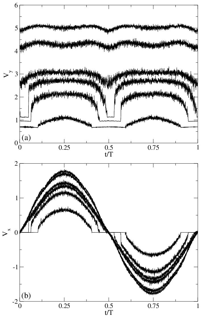
(b) From bottom to top, A = 0.43, 0.5, 0.6, 0.75, 1.0, 1.5, and 2.5.
Symmetry locking of the type shown in Fig. 10(b) for high drives has been observed previously both for vortices moving over periodic substrates [19] and in experiments on colloids moving over a square substrate [56]. In the colloidal studies, the dynamical locking occurred in the single particle limit, so the order-disorder type behavior we observe did not occur. We expect that for denser colloidal assemblies when a colloidal crystal forms, it should be possible to observe the order-disorder phenomena we describe here.

C.  Commensurability Effects Near the B/Bϕ = 2.0 State

We next examine commensurability effects near the ordered dimer state. In Fig. 18(a) we plot Vx for B/Bϕ = 1.89 for a system with the same parameters as Fig. 1 where we observed polarization switching of the dimer state. At the incommensurate filling, the large interstitial pins contain a mixture of dimers and monomers and the global orientational ordering of the dimers is lost. Those dimers that are present form some local ferromagnetic order in one of the three symmetry directions. Under an applied ac drive, a portion of the dimers align with the drive; however, the overall disorder in the sample creates randomness in the energy barriers that a dimer must overcome to switch to a new orientation. This randomness destroys the sharp global switching of the dimers shown in Fig. 3 at B/Bϕ = 2.0 and replaces it with a series of smaller avalanche-like switching events. This is illustrated in Fig. 18(a) where only a portion of the dimers change orientation in any switching event. In Fig. 19(a) we show a time trace of the vortex trajectories for the system in Fig. 18(a) over several ac drive periods, illustrating that the interstitial dimers and monomers remain pinned but can move within each large interstitial region. The resulting trajectories are much more random than in the B/Bϕ = 2.0 switching case shown in Fig. 2. The switching pulses in Fig. 18(a) do not follow the same pattern for successive periods, indicating that the avalanche pattern is different from one period to another and has chaotic-like features. This type of chaotic avalanche behavior is very similar to the Barkhausen noise effects found in disordered spin systems [57]. A fuller examination of the Barkhausen or crackling noise effect observed in Fig. 18(a) will be presented in a later work.
For B/Bϕ = 2.056, there is a mixture of dimers and trimers in the large interstitial regions, and for A = 0.075, a partial depinning of the interstitial vortices occurs creating the large velocity bursts shown in Fig. 18(b). The bursts are generally confined to regimes where the particles can channel along the six easy-flow directions of the pinning lattice, as illustrated in Fig. 19(b). For lower values of A, the partial depinning is lost and the system has a random switching behavior similar to that shown in Fig. 18(a). For very low ac amplitude, even the random switching is lost and the dimers and trimers remain locked in a fixed orientation.
Fig18.png
Figure 18: (a) Vx vs time for a system with the same parameters as in Fig. 2 with A=0.075, but with B/Bϕ = 1.89. The vortices all remain pinned and the switching from one dimer orientation to another is random and reminiscent of Barkhausen noise. (b) Vx versus time for the same system with B/Bϕ = 2.056, where a portion of the vortices begin to slide as the drive is rotated.
Fig19.png
Figure 19: Vortex positions (filled dots), pinning site locations (open circles), and vortex trajectories (lines) during several periods of motion. (a) The system in Fig. 18(a) at B/Bϕ = 1.89. The interstitial vortices follow disordered closed orbits. (b) The system in Fig. 18(b) at B/Bϕ=2.056. The interstitial vortices depin and move from one interstitial region to another, while the vortices at the pinning sites remain pinned.

D.  ac Effects on the Vortex Trimer State at B/Bϕ = 2.5

As a function of field, higher order vortex molecular crystal states form whenever orientationally ordered n-mer states occur, such as at B/Bϕ = 2.5, 3.0, or 3.5. These states can show a polarization effect as a function of the external drive similar to that observed for B/Bϕ = 2.0. We focus on the case of B/Bϕ = 2.5, where the large interstitial regions each capture three vortices per pinning site and the trimers have a ferromagnetic ordering [45]. When the external drive is small, the trimers remain locked in one orientation without switching. For larger ac drives, switching of the trimer orientation occurs that is similar to the switching observed for the dimers. For even larger ac drives, a new type of switching effect occurs for the trimers that is absent for the dimer system. Within the large interstitial site, the three vortices in the trimer form a triangle. When the trimer is aligned along θ = π/2 as in Fig. 5(c) of Ref. [45] and the ac drive is also aligned along θ = π/2, the vortex at the top of the triangle experiences an extra force from the lower two vortices in the triangle and depins into the interstitial site above. The same process occurs at every large interstitial site and so there is an exchange of one vortex from each site to the site above. The net result is that the trimers reverse their orientation and are now pointing along θ = 3π/2. The new orientation is more stable against depinning by the external drive. The two vortices at the top of the reoriented trimer produce a barrier for the motion of the vortex at the bottom of the trimer. At the same time, the top two vortices are too wide to hop out of the interstitial site into the interstitial site above. This can be regarded as a jamming effect. As the ac drive cycle continues, the drive rotates into the θ = 3π/2 direction, and the lower vortex in each trimer can jump into the interstitial site below, reorienting the trimer to point along θ = π/2. Thus in this phase, trimer reorientation occurs by the exchange of individual vortices between neighboring interstitial sites, rather than by the rotation of the trimer itself. For higher ac drives, a sliding state appears when the vortices move along the symmetry directions of the pinning lattice.
In Fig. 20 we plot Vy versus time for different values of A in a system at B/Bϕ = 2.5 with the same parameters as in Fig. 1. At this filling a set of phases appear which are similar to those found at B/Bϕ = 2.0. At very low A, the trimers are pinned, while for larger A the system has sliding states interlaced with pinned states. A strong channeling effect produces local maxima and minima in Vy, similar to the B/Bϕ = 2.0 system. For A < 0.15, the vortices at the pinning sites remain pinned and a local minimum in |Vy| occurs at t/T=0.5. For A > 0.15 this minimum turns into a maximum when the vortices in the pinning sites begin to depin and generate a random flow phase. For A = 0.3, the transition from a locked flowing phase of interstitial vortices to the random phase produces a large jump in Vy. In general, we find that as B/Bϕ increases, a more complicated set of features in the velocity force curves appears.
Fig20.png
Figure 20: Vy vs time for a system with the same parameters as in Fig. 2 but with B/Bϕ = 2.5, where a trimer state forms. From lower left to upper left, A = 0.075, 0.1, 0.125, 0.15, 0.25, 0.3, and 0.4. For A < 0.15 there is a minimum in |Vy| at t/T=0.5, while for A ≥ 0.25 a maximum in |Vy| begins to form at t/T=0.

IV.  FIXED DC DRIVE IN THE Y-DIRECTION WITH AN AC DRIVE IN THE X-DIRECTION

In previous work on a honeycomb pinning array at B/Bϕ = 2.0, we found that when a dc drive is applied in the x-direction, the vortices flow along either θ = π/6 or θ = −π/6 depending on the original orientation of the dimers in the ground state at Fd=0 [46,47]. Once the dimers are flowing under the dc drive, application of an additional ac drive in the y direction can induce a switching between flow along θ = π/6 and θ = −π/6 [46]. There is a threshold amplitude of the ac drive required to cause the switching in the symmetry breaking flow states. Here we consider the case of a dc drive Fdc=Fdcy fixed in the y direction with an ac drive Fac = Asin(2πt/T)x. applied in the x direction. For A = 0, the dimers flow in one-dimensional paths along the y direction and there is no symmetry breaking of the flow, unlike the symmetry broken flow that occurs for an x direction dc drive. When an additional ac drive is applied in the x direction, transverse to the dc drive, the average value of Vy can be strongly influenced.
In Fig. 21 we plot Vx and Vy versus time for a system at B/Bϕ=2.0 with a y direction dc drive of Fdc=0.15 and an x direction ac drive with A = 0.35. For 0 < t/T < 0.075, the dimer motion is locked along θ = π/2. Although the magnitude of the ac drive is increasing in the positive x direction during this time period and therefore the overall net driving force vector is increasing in magnitude, Vy decreases monotonically with time until a switching event occurs at t/T=0.075 when the dimers transition from flowing along θ = π/2 to flowing along θ = π/6. This switch coincides with a sharp jump in Vx to a positive value and a cusp feature in Vy. After the switching event, Vx and Vy gradually increase with time until t/T=0.25, when they begin to decrease. For 0.075 ≤ t/T ≤ 0.4, the value of Vy is higher than it would be under only a dc force and no ac force, indicating that the application of a perpendicular ac drive can increase the velocity in the direction of the dc drive. For 0.25 < t/T < 0.5, both Vx and Vy decrease until Vx = Vy = 0, indicating that the system is pinned. The ac drive begins to increase in the negative x direction above t/T=0.5, and as the dimers reorient to follow the net drive vector they realign with θ = π/2 and are once again able to slide along θ = π/2 for 0.525 < t/T < 0.58. At t/T=0.58, another switching event occurs and the dimers slide along θ = 11π/6.
Fig21.png
Figure 21: Vx (dark line) and Vy (light line) versus time for a system at B/Bϕ=2.0 with a y direction dc drive of Fdc = 0.15 and an x direction ac drive with A = 0.35. At t/T=0, the dimers are moving along θ = π/2. At t/T=0.075, a switching transition occurs and the dimers slide along θ = π/6. Near t/T=0.5, a pinned phase (P) appears. This shows that the application of an ac drive induces a pinned phase in a system with a dc drive. We note that the ac drive amplitude is zero at t/T=0.5 and the pinned phase occurs due to the reorientation of the dimers by the ac drive into a jammed configuration that is perpendicular to the dc drive. We call this the jamming transistor effect.
We term the pinning effect in Fig. 21 near t/T=0.5 a jamming transistor effect. At t/T=0.5, the ac force is zero in the x-direction, so Vy would be expected to take the value it had at t/T=0 when the ac force was also zero. Instead, Fig. 21 shows that Vy=0 at t/T=0.5. At this point, the ac drive has reoriented the dimers so that they are aligned along θ = 0, instead of along θ = π/2 as they were at t/T=0. In previous work on honeycomb pinning arrays at B/Bϕ = 2.0, we showed that if a dc drive is applied in the y-direction and the dimers are aligned perpendicular to the applied driving force, an unusually high critical depinning force appears due to the fact that the dimers are effectively jammed [47]. The pinned phase near t/T=0.5 in Fig. 21 is an example of this jamming effect. The dimers act like rigid objects and cannot move through the y-direction channel between adjacent interstitial pinning sites unless they are aligned along θ = π/2. A key difference between the effect described here and the jamming in our previous work is that the jamming in Ref. [47] occurred as an equilibrium transition in the ground state when the pinning force was increased. In the present case, the dimers are reoriented dynamically. In Fig. 22 we schematically illustrate the dynamic jamming effect. In Fig. 22(a), a dimer oriented along θ = π/2 can move between the pinning sites and has a low depinning threshold. If the dimer is oriented along θ = 0 as in Fig. 22(b), parallel to the two pinning sites, the energy barrier for the dimer to pass between the pinning sites is much higher and the depinning force is correspondingly higher.
Fig22.png
Figure 22: Schematic of the jamming effect. Light circles: dimer vortices in interstitial site. Dark circles: pinned vortices. Open circles: pinning sites. (a) A dimer oriented along θ = π/2 can easily move between two occupied pinning sites and has a low depinning threshold. (b) A dimer oriented along θ = 0 has difficulty moving between the occupied pinning sites, and the depinning threshold is much higher.
In Fig. 23 we plot Vx and Vy for a system containing only interstitial monomers at B/Bϕ=1.5 under the same drive configuration as in Fig. 21, with a dc drive applied in the y-direction and an ac drive applied in the x-direction. There is a modulation in Vy, with a dip near t/T=0.12 at the point where Vx rises above zero; however, Vy never drops to zero and there is no pinned phase. At t/T=0.5, Vy reaches the same value it had at t/T=0 at the beginning of the period when the ac drive component was zero. This is distinct from the behavior of the dimer system, where Vy dropped to zero at t/T=0.5 due to the reorientation of the dimers. We find behavior similar to that shown in Fig. 23 over a wide range of ac and dc drive parameter values for B/Bϕ=1.5. In general, the application of a force in the x-direction to a system of monomers being driven in the y direction does not induce a pinned phase or a phase where Vy = 0. The fluctuations in Vy increase when Vx becomes finite because the flow in this regime is disordered, although the vortices at the pinning sites remain pinned. The monomers randomly alternate which side of the occupied pinning sites they move around.
Fig23.png
Figure 23: Vx (dark line) and Vy (light line) for the same system in Fig. 21 with B/Bϕ = 1.5 so that no dimers are present. The dc drive is in the y direction with Fdc = 0.425 and a sinusoidal ac drive is applied in the x direction with A = 0.35. Unlike the case of B/Bϕ = 2.0, the velocity responses at t/T=0 and t/T=0.5 are the same.

A.  Jamming Transistor Effect

A system in which a dc velocity component can be switched on and off with an ac drive applied perpendicular to the dc drive has similarities to field effect transistor devices. The strong cusp in Vy near t/T=0.075 in Fig. 21 and the corresponding sudden jump in Vx suggest that the rapid switching time could be used to create semiconductor type devices similar to the transverse field effect depinning threshold modulation in charge density wave systems [48,49]. Since the external ac field can control the dimer orientation and since the depinning threshold depends on the orientation of the dimers, the system should exhibit strong memory effects of its original configuration. For example, different settings of the initial ac and dc drive values would orient the dimers in a particular direction and the pinning threshold would depend on the history of the preparation of the dimer states. These field effect type properties could be useful for making vortex-based devices or could be used as models for constructing similar systems on smaller scales using ions or Wigner crystals.
We showed in Fig. 23 that monomers do not exhibit a jamming effect. In general, the jamming effect occurs when B/Bϕ is close to B/Bϕ = 2.0. As long as there are enough interstitial dimers to percolate throughout the entire sample, the dimers can induce a jamming effect which has a side effect of pinning any monomers or trimers that are present. Even at B/Bϕ = 2.0, there is a threshold value of Fdc above which the jamming transition no longer occurs, as we describe in Section IV C. For fields away from B/Bϕ = 2.0, this dc threshold force is reduced. For B/Bϕ < 1.75, a complete jamming effect is lost; however, portions of the system populated with dimers can still jam. For B/Bϕ < 2.0 and low enough Fdc, the monomers are simply pinned at the interstitial sites and jamming of the dimers has no effect on the monomer pinning.

B.  Varied ac Amplitude and Fixed dc Amplitude

We next examine the effect of varied ac amplitude for a system with fixed Fdc = 0.1 applied in the y direction at B/Bϕ = 2.0. If the ac amplitude is too small, the vortex motion remains locked along θ = π/2 in the y-direction. In Fig. 24(a) we plot Vx and Vy for A = 0.16. At this ac drive value, the jump in Vx is close to its maximum amplitude, and the corresponding cusp feature in Vy is reduced in size. The pinned phase near t/T=0.5 is also more extended than in the sample illustrated in Fig. 21. In Fig. 24(b) we show Vx and Vy in the same system at A = 0.15, which is just below the ac threshold required to unlock the motion from the y-direction, θ = π/2. In this case Vx = 0 throughout the cycle while Vy has a periodic modulation but is always finite. Even though the vortices are not translating in the x-direction, the application of an ac force in the x-direction causes the vortices flowing along the y direction to shift toward one side of the θ = π/2 flow channel. This increases the strength of the interaction between the moving vortices and the pinned vortices and increases the effective drag on the moving vortices, reducing Vy whenever the absolute value of the ac drive is maximum in the positive or negative x-direction. In Fig. 25 we show a series of Vy versus time curves for increasing ac drive amplitude with A = 0.35, 0.45, 0.55, and 0.85. As A increases, the transition from θ = π/2 to θ = π/6 motion occurs at earlier t/T. For A > 0.35, there is a large jump into a fluctuating phase centered near t/T=0.25, corresponding to the depinning of a portion of the pinned vortices into a random flow regime. The system can then reorganize to the θ = π/6 flow phase at a later point in the period when the force from the ac drive goes to zero and the net driving force is no longer large enough to depin vortices from the pinning sites. The vortices enter a pinned phase at t/T=0.5.
Fig24.png
Figure 24: (a) Vx (dark line) and Vy (light line) vs time for a system with a y direction dc force of Fdc = 0.15 and an x direction ac force with A = 0.16. Here the jamming transition appears along with a strong switching effect in Vx. (b) The same system at A = 0.15, where the ac amplitude is too small to induce a switching effect and Vx=0.
Fig25.png
Figure 25: Vy vs time for the same system in Fig. 21 with Fdc=0.15 at A = 0.35, 0.45, 0.55, and 0.85, from bottom to top. The large jump for A > 0.35 near t/T=0.25 is the onset of the random phase where vortices at the pinning states start to depin.
In Fig. 26 we show the dynamical phase diagram of time versus ac amplitude A during half of the ac drive period with fixed Fdc=0.15. At small t/T when the ac force is first increasing from zero, the system always starts with the dimers flowing along θ = π/2. For decreasing A, the temporal extent of the θ = π/2 region grows until for A ≤ 0.15 the system is always locked to θ = π/2, as shown in Fig. 24(b) for A = 0.15. For 0.15 < A < 0.45, the system passes through θ = π/2 and θ = π/6 locked flow phases and a jammed or pinned phase in half a period. The random flow phase first appears for A ≥ 0.45. In the random flow phase, vortices at the pinning sites depin when the net driving force from the combined dc and ac drives is maximum, which occurs at t/T=0.25. The jammed phase which is centered at t/T=0.5 becomes narrower but still persists for increasing A. For A > 1.25 (not shown) there are new types of moving phases that arise within the random phase region when all the vortices depin and start sliding along the pinning sites, producing the order-disorder transitions studied earlier.
Fig26.png
Figure 26: The dynamical phase diagram for time t/T vs ac amplitude A for the system in Fig. 21 with a fixed dc drive of Fdc=0.15 in the y-direction and an ac drive applied in the x-direction. In the θ = π/2 phase the dimers flow along the y-direction, while for higher A they flow along θ = π/6. The pinned phase is marked P while R is the random phase where the vortices start to depin from the pinning sites.

C.  Constant ac Amplitude and Varied dc Amplitude

We next consider the case where the x direction ac drive amplitude is fixed at A=0.2 and the y direction dc drive amplitude is varied at B/Bϕ = 2.0. At Fdc = 0, the behavior of the system resembles that observed in earlier studies with only a dc drive in the x-direction [46,47]. In this limit the ac drive applied along the x direction induces flow along θ = π/6 or θ = 11π/6, with the flow reversing during the second half of the ac cycle to θ = 7π/6 or θ = 5π/6, respectively. In Fig. 27(a) we plot Vx and Vy for a system with Fdc = 0 and A = 0.2. Here the vortices are initially pinned and then undergo a transition to the moving θ = 11π/6 phase. In this case, the dimers were oriented along θ = 11π/6 in the initial pinned ground state. The amplitude of Vx is larger than Vy since |Vx| = |Acos(11π/6)| and |Vy| = |Asin(11π/6)|. When the ac drive reverses, the dimers flow along θ = 5π/6. The symmetry breaking of the dimers in the ground state fixes the flow direction of the dimers for all later times. If we consider an incommensurate case where there are additional disordered phases, the system dynamically organizes into one of the broken symmetry phases. In this case, when the ac drive reverses sign, the system passes though the disordered phase which destroys the memory of the dynamically broken symmetry phase, and the vortices have an equal chance of dynamically breaking symmetry in either of the two possible directions.
Fig27.png
Figure 27: Vx (dark line) and Vy (light line) vs time for a system at B/Bϕ = 2.0 with a y direction dc drive and an x direction sinusoidal ac drive with A = 0.2. (a) Fdc = 0. Here the vortex motion is locked along θ = 11π/6 or 5π/6 during a portion of the first and second halves of each ac drive cycle. (b) Fdc=0.05. Here, the dc drive is not strong enough to lock the motion to only the positive y-direction, and the direction of motion is determined by the symmetry breaking of the dimers in the ground state.
At B/Bϕ = 2.0, if a small but finite dc drive Fdc is applied in the y direction, it is unable to break the symmetry of the ground state, and the ground state dimer orientation determines the resulting dynamics, as illustrated in Fig. 27(b) for a system with Fdc = 0.05. Here the vortices are initially pinned and then depin to flow along θ = π/6, reflecting the orientation of the dimers in the pinned state. During the second half of the drive period, the dimers flow along 7π/6 and |Vx| and |Vy| are both lower than they were during the first half of the drive period. This is due to the biasing force of the dc drive component which is applied in the positive y direction. When Fdc is sufficiently strong, the negative component of the y velocity during the second half of the drive period is lost.
In Fig. 28 we plot Vy versus time for A = 0.2 and Fdc = 0.05, 0.125, 0.2, 0.225, and 0.275. For Fdc > 0.125, Vy is always positive. For Fdc > 0.1, the vortices initially move along θ = π/2 and as Fdc increases, the magnitude of Vy increases, as does the magnitude of the jump from θ = π/6 back to θ = π/2 near t/T=0.5. At Fdc = 0.275, the θ = π/6 phase is replaced with a randomly fluctuating phase when the net force from the combined dc and ac drives is strong enough to depin vortices from the pinning sites, similar to the behavior shown earlier. For Fdc < 0.2, Vx (not shown) steadily rises with t/T and reaches a maximum value near t/T=0.25 which saturates for Fdc > 0.2. The saturation occurs since the ac component in the x-direction is fixed. The onset of the random phase also produces increased fluctuations in Vx at Fdc = 0.275.
Fig28.png
Figure 28: Vy vs time for the same system in Fig. 27 with an x direction ac drive of A = 0.2 and a y direction dc force. From bottom to top, Fdc = 0.05, 0.125, 0.2, 0.225, and 0.275. The onset of the random phase where vortices depin from the pinning sites appears as a jump into a strongly fluctuating phase for the Fdc = 0.275 curve.
In Fig. 29(a) we show the continued evolution of Vy from Fig. 28(a) for Fdc = 0.33, 0.41, 0.45, 0.5, 0.55, and 0.6. The θ = π/2 sliding phase diminishes in size with increasing Fdc and vanishes completely for Fdc > 0.475 while the random flow phases grow in extent. Within the random flow phases for Fdc > 0.475, there is a modulation of Vy with dips near t/T=0, t/T=0.5, and t/T=1, along with smaller modulations near t/T=0.25 and t/T=0.75. It is interesting to note that the ratio of Vy at t/T=0.25 to Vy at t/T=0.5 reaches a maximum at Fdc = 0.45. Here Vy is strongly reduced when the system enters the θ = π/2 phase because the vortices that depinned during the random flow phase repin in the θ = π/2 phase and no longer contribute to Vy. In Fig. 29(b) we show the corresponding Vx curves which indicate that the θ = π/2 locked flow phase disappears for Fdc > 0.475.
Fig29.png
Figure 29: (a) Vy vs time for the system in Fig. 28 at A = 0.2 and Fdc = 0.33, 0.41, 0.45, 0.5, 0.55, and 0.6 (from bottom to top). For Fdc > 0.45, the sliding phases θ = π/2 at t/T=0 and t/T=0.5 are lost. (b) The corresponding Vx vs time at Fdc=0.33, 0.41, 0.45, 0.5, 0.55, and 0.6 (from bottom to top at t/T=0).
In Fig. 30 we plot the dynamic phase diagram for Fdc versus time at fixed A = 0.2 for the system in Figs. 28 and Fig. 29 at B/Bϕ=2.0. For t/T < 0.1 and Fdc < 0.075, the vortices are initially in the pinned phase. As t/T increases and the ac force becomes larger, the vortices organize into a pinned symmetry broken state for Fdc < 0.075 or depin into the θ = π/6 sliding state for 0.075 ≤ Fdc < 0.475. The initial pinned state is lost for Fdc > 0.1 when the dc drive is strong enough to cause the dimers to slide along θ = π/2. For Fdc > 0.475, the dc drive combined with the motion of the interstitial vortices is strong enough to depin the vortices at the pinning sites and the system enters the random phase even when Fac = 0 at t/T=0. For 0.1 ≤ Fdc ≤ 0.25, the system switches from θ = π/2 to θ = π/6 dimer flow, while the θ = π/6 phase is lost for Fdc ≥ 0.25 and the system enters the random flow state. The second pinned state near t/T=0.5 disappears for Fdc > 0.2. Due to the polarization of the dimers, this is higher than the drive at which the pinned state disappears for t/T=0. For higher dc amplitudes than those shown in Fig. 30, all of the vortices depin and slide along certain directions of the pinning lattice, forming the order-disorder transitions studied earlier.
Fig30.png
Figure 30: Dynamic phase diagram Fdc versus time for the same system in Figs. 28 and Fig. 29 at B/Bϕ=2.0 under an x direction ac drive with A = 0.2 and a y direction dc drive. P: pinned phase; SB: symmetry breaking phase where the symmetry is broken in the pinned dimer configuration; R: random phase where vortices at the pinning sites become depinned. There are two sliding phases along θ = π/2 and θ = π/6.

D.  Commensurability Effects

We next consider the effects of varied B/Bϕ. Figure 31 shows Vy versus time for B/Bϕ = 2.44, 3.0, 3.4, and 4.72 for a system with fixed Fdc = 0.35 applied in the y-direction and an ac force with A=0.2 applied in the x-direction. For clarity, the velocities are normalized by the value of Vy at B/Bϕ = 2. For B/Bϕ = 2.44, the system is in the random phase throughout the driving period; however, a prominent channeling effect persists as shown by the minima at t/T=0.5 and t/T=1.0 as well as the smaller shoulders at t/T=0.25 and t/T=0.75. For B/Bϕ = 3.0, the system forms several new ordered flow phases visible as regions of reduced fluctuations in Vy. The ordered interstitial flow phase ends at t/T=0.04 with a transition into a random flow regime, as shown by the drop in Vy. The same ordered interstitial flow state reappears just before and after t/T=0.5, as indicated by the sharp cusps in Vy, and also occurs for B/Bϕ = 3.4. In Fig. 32 we illustrate the vortex trajectories in the ordered interstitial flow phase for B/Bϕ = 3.4. The moving interstitial vortices channel in periodic winding paths at an angle between the occupied pinning sites. At this particular filling, a small portion of the interstitial vortices are trapped behind the occupied pinning sites. The ordered interstitial flow phase at B/Bϕ=3.0 is nearly identical except that the immobile interstitial vortices are not present.
Fig31.png
Figure 31: Vy vs time at varied B/Bϕ with a y direction dc drive of Fdc = 0.35 and an x direction ac drive with A = 0.2. For clarity, the velocities are normalized by the value of Vy at B/Bϕ = 2.0. From top to bottom, B/Bϕ = 2.44, 3.0, 3.4, and 4.72. For B/Bϕ = 3.4, a complex cusp structure forms and two different types of ordered phases appear.
Fig32.png
Figure 32: Vortex positions (filled dots), pinning site locations (open circles), and vortex trajectories (lines) in the ordered interstitial flow phase at t/T=0.025 for the B/Bϕ = 3.4 system in Fig. 31. Here the moving interstitial vortices form ordered channels between the pinning sites. A small portion of the interstitial vortices are pinned behind occupied pinning sites. This same type of ordered interstitial flow phase occurs at B/Bϕ=3.0.
In Fig. 31, as the ac force increases for B/Bϕ = 3.0 the vortices at the pinning sites depin into a floating triangular structure and the flow becomes random at t/T=0.1. Near t/T=0.15, the fluctuations in Vy are reduced when a portion of the vortices lock into a channeling motion along the pinning rows. For B/Bϕ = 3.4, the same floating triangular lattice appears; however, the transition from the random phase to the channeling phase centered at t/T=0.25 is much sharper. The plot of P6 versus time for the B/Bϕ=3.4 system in Fig. 33 shows the transition to the floating triangular state, and also indicates that the vortex lattice regains some order during the ordered interstitial flow phases. The transitions into the disordered regimes appear as drops in P6.
Fig33.png
Figure 33: The fraction of six-fold coordinated vortices P6 vs time for the B/Bϕ = 3.4 system from Fig. 31. The cusp structures in Vy in Fig. 31 correlate with the features in P6. In the channeling phase centered at t/T=0.25, the vortices form a mostly triangular lattice.
For B/Bϕ = 4.72 in Fig. 31, random flow phases dominate the behavior; however, several cusp features still appear in Vy. The vortex lattice is also mostly triangular near t/T=0.25. A new feature at this field is the transformation of the minima in Vy at t/T=0.5 into a small maximum. These results show that there is a complex variety of phases at the different fields which have clear transport and ordering signatures.

V.  MODIFIED VORTEX INTERACTIONS FOR THIN FILM SUPERCONDUCTORS

In the previous sections we considered vortex-vortex interactions which are appropriate for bulk superconductors. In many cases, however, periodic pinning experiments are carried out using thin film superconductors where the vortices interact with the logarithmic Pearl potential [59]. Previous simulations for vortices interacting with periodic pinning arrays using the logarithmic vortex-vortex interaction potential [60,11] have found similar commensurability effects and dynamics as those in simulations with bulk vortex-vortex interactions [10,19,45,46,61].
Fig34.png
Figure 34: Vx (dark line) and Vy vs time for a system at B/Bϕ = 2.0 with a fixed dc drive of Fdc=0.15 in the y-direction and an ac drive with A=0.2 in the x-direction. Here the vortex-vortex interaction potential is of a logarithmic form appropriate for a thin film superconductor. We observe the same jamming transition effect described in Section IV for vortices with a bulk interaction potential, indicating that the effect is robust for thin-film superconductors.
To test the effects of the different vortex-vortex interactions on the honeycomb pinning system, we revisit the jamming transistor effect described in Section IV at B/Bϕ=2.0 where a fixed dc drive causes the vortices to channel along the y direction and an ac drive is applied in the x direction. We take the total force of the vortex-vortex interaction in Eq. (1) to be
Fivv=− Nv

ji 
AviUv(Rij)
^
R
 

ij 
(5)
where U(r)=−ln(r), the Pearl vortex-vortex interaction potential appropriate for thin-film superconductors. Here Av = ϕ02/8πΛ, where Λ is the effective two-dimensional penetration depth for a thin film superconductor. We compute the vortex-vortex interaction force using a real-space Lekner summation technique to deal effectively with the long range interaction in a periodic system [62,63]. We conduct the same type of simulation as in Section IV for a system with a y direction dc drive of Fdc = 0.15 and an x direction ac drive with A = 0.2. In Fig. 34 we plot the resulting Vx and Vy versus the ac drive period. The same features occur as in the case of vortices with a bulk interaction, including the jamming transistor effect in which Vy can be brought to zero due to the rotation of the dimers. The key ingredient for observing the effects described throughout this paper is that the vortices must form interstitial n-mer states due to the combination of interstitial trapping and repulsive vortex interactions, regardless of the nature of the vortex interaction potential. One difference that we find between logarithmic and bulk interactions is that for the logarithmic interactions, when the system passes from the disordered flow phase to the ordered flow phase, the channeling of the vortices still occurs but is not as coherent as in the bulk interaction case. This may be due to the smaller shear modulus of the vortex lattice with the thin-film interaction potential. All of the general features of the disordered to ordered flow transition are preserved for either potential.
Fig35.png
Figure 35: Vortex positions (filled dots), pinning site locations (open circles), and vortex trajectories (lines) during several drive periods for the same system in Fig. 23 with a y direction dc drive of Fdc=0.425 and an x direction ac drive with A=0.35. In Fig. 23 the frequency was 103 times lower and the system exhibited a switching from θ = π/2 flow to θ = π/6 flow. Here, the ac frequency is higher than the ability of the vortices to respond, and the motion stays locked in the θ = π/2 direction.

VI.  DISCUSSION

In this work we considered varied ac drive amplitude but kept the ac drive frequency fixed. Our results should be robust in the low frequency regime, and for frequencies lower than the frequency considered here, the results do not change. At much higher frequencies, the system does not have time to respond to the ac drive and the switching events will be lost. In our previous work, we found that for a frequency about 10 to 100 times higher than the frequency considered here, the system stops responding to the ac drive [46]. In Fig. 35 we show an example of this effect for a system with a dc drive applied in the y-direction and an ac drive applied in the x-direction, with the same parameters as the system in Fig. 23 but at a higher frequency. For low frequency, the system shows a switching effect from θ = π/2 flow to θ = π/6 flow. In Fig. 35 the frequency is 103 times higher and the vortex trajectories show oscillations; however, the net motion remains locked to θ = π/2.
Our previous work with this system showed that temperature effects can change the phase boundaries slightly, but that the ordered dynamical phases persist until the melting transition of the interstitial vortices is reached [46,47]. In the present work, we focused on the limit where the pinning is strong enough that there is a regime in which the vortices at the pinning sites can remain pinned while the interstitial vortices flow. As Fp decreases, many of the dynamical phases will disappear as the dimers lose their independent effective orientational degree of freedom. For low enough Fp, additional transitions can occur in the vortex lattice where a portion of the formerly pinned vortices are no longer located at the pinning sites, producing a triangular structure [32,45,58].

VII.  SUMMARY

We have shown that in honeycomb pinning arrays, vortex molecular crystalline states which have effective orientational degrees of freedom can have their orientation controlled by an external ac drive. We specifically focused on vortex dimers at the second matching field which have three different possible orientations. When an ac drive is applied in both the x and y directions, the orientation of the dimers can be made to follow the external drive while the vortices remain pinned in the large interstitial site. We term this a polarization effect. In this regime the dimers rotate by a combination of continuous motion and a switching type behavior that appears as large velocity jumps when the dimers switch to the different symmetry angles of the pinning array. For very weak ac drive amplitudes, the dimers remain locked in their initial orientation, showing that there is a threshold force needed to induce the pinned switching behavior. For large ac drive amplitudes, the dimers depin and flow between the pinned vortices along certain symmetry directions of the pinning lattice, producing distinctive features in the x and y components of the velocity during each ac period. For even larger ac drive amplitudes, all the vortices depin and the system exhibits a series of order-disorder transitions and symmetry locking effects as a function of ac drive. We also consider the case of a fixed dc drive applied in one direction and an ac drive applied in the perpendicular direction. Here, the application of the ac drive can cause the moving dimers to orient in such a way that they become effectively jammed. We call this effect a jamming transistor and show that it occurs due to the fact that the dimers can slide more easily if they are oriented along the symmetry axis of the pinning rows. The ac drive can also induce a pronounced dynamical switching that can be seen in both velocity components. Many of the switching features may be useful for creating new types of vortex based devices or fluxtronics, and can serve as examples for other systems in which molecular crystal type states can form, such as ions or Wigner crystals on periodic substrates, colloidal molecular crystals, or vortices in Bose-Einstein condensates.

  ACKNOWLEDGMENTS

We thank M. Hastings for useful discussions. This work was carried out under the NNSA of the U.S. DOE at LANL under Contract No. DE-AC52-06NA25396.

References

[1]
E.H. Brandt, J. Low. Temp. Phys. 53, 41, 71 (1983); H.J. Jensen, A. Brass, and A.J. Berlinsky, Phys. Rev. Lett. 60, 1676 (1988); H.J. Jensen, A. Brass, Y. Brechet, and A.J. Berlinsky, Phys. Rev. B 38, 9235 (1988).
[2]
A.E. Koshelev and V.M. Vinokur, Phys. Rev. Lett. 73, 3580 (1994).
[3]
P. Le Doussal and T. Giamarchi, Phys. Rev. B 57, 11 356 (1998).
[4]
L. Balents, M.C. Marchetti, and L. Radzihovsky, Phys. Rev. Lett. 78, 751 (1997); Phys. Rev. B 57, 7705 (1998).
[5]
K. Moon, R.T. Scalettar, and G.T. Zimányi, Phys. Rev. Lett. 77, 2778 (1996); S. Spencer and H.J. Jensen, Phys. Rev. B 55, 8473 (1997); C.J. Olson, C. Reichhardt, and F. Nori, Phys. Rev. Lett. 81, 3757 (1998); A.B. Kolton, D. Domínguez, and N. Grønbech-Jensen, ibid. 83, 3061 (1999).
[6]
S. Bhattacharya and M.J. Higgins, Phys. Rev. Lett. 70, 2617 (1993); A.C. Marley, M.J. Higgins, and S. Bhattacharya, ibid. 74, 3029 (1995).
[7]
F. Pardo, F. de la Cruz, P.L. Gammel, E. Bucher, and D.J. Bishop, Nature (London) 396, 348 (1998); A.M. Troyanosvki, J. Aarts, and P.H. Kes, ibid. 399, 665 (1999).
[8]
E. Olive and J.C. Soret, Phys. Rev. B 77, 144514 (2008).
[9]
N. Mangan, C. Reichhardt, and C.J. Olson Reichhardt, Phys. Rev. Lett. 100, 187002 (2008).
[10]
C. Reichhardt, C.J. Olson, and F. Nori, Phys. Rev. Lett. 78, 2648 (1997); Phys. Rev. B 58, 6534 (1998).
[11]
C. Reichhardt, G.T. Zimányi, and N. Grønbech-Jensen, Phys. Rev. B 64, 014501 (2001).
[12]
G. Carneiro, Phys. Rev. B 62, R14 661 (2000); 66, 054523 (2002).
[13]
B.Y. Zhu, L. Van Look, V.V. Moshchalkov, B.R. Zhao, and Z.X. Zhao, Phys. Rev. B 64, 012504 (2001).
[14]
K. Harada, O. Kamimura, H. Kasai, T. Matsuda, A. Tonomura, and V.V. Moshchalkov, Science 274, 1167 (1996).
[15]
E. Rosseel, M. Van Bael, M. Baert, R. Jonckheere, V.V. Moshchalkov, and Y. Bruynseraede, Phys. Rev. B 53, R2983 (1996).
[16]
C. Reichhardt, R.T. Scalettar, G.T. Zimányi, and N. Grønbech-Jensen, Phys. Rev. B 61, R11 914 (2000).
[17]
M. Vélez, D. Jaque, J.I. Martín, F. Guinea, and J.L. Vicent, Phys. Rev. B 65, 094509 (2002).
[18]
R. Surdeanu, R.J. Wijngaarden, R. Griessen, J. Einfeld, and R. Wördenweber, Euorphys. Lett.  54, 682 (2001).
[19]
C. Reichhardt and F. Nori, Phys. Rev. Lett. 82, 414 (1999).
[20]
M. Velez, D. Jaque, J.I. Martín, M.I. Montero, I.K. Schuller, and J.L. Vicent, Phys. Rev. B 65, 104511 (2002).
[21]
A.V. Silhanek, L. Van Look, S. Raedts, R. Jonckheere, and V.V. Moshchalkov, Phys. Rev. B 68, 214504 (2003).
[22]
J.E. Villegas, E.M. Gonzalez, M.I. Montero, I.K. Schuller, and J.L. Vicent, Phys. Rev. B 72, 064507 (2005).
[23]
T.C. Wu, P.C. Kang, L. Horng, J.C. Wu, and T.J. Yang, J. Appl. Phys. 95, 6696 (2004).
[24]
Z. Jiang, D.A. Dikin, V. Chandrasekhar, V.V. Metlushko, and V.V. Moshchalkov, Appl. Phys. Lett. 84, 5371 (2004).
[25]
Q.H. Chen, C. Carballeira, T. Nishio, B.Y. Zhu, and V.V. Moshchalkov, Phys. Rev. B 78, 172507 (2008).
[26]
A.T. Fiory, A.F. Hebard, and S. Somekh, Appl. Phys. Lett. 32, 73 (1978).
[27]
V.V. Metlushko, M. Baert, R. Jonckheere, V.V. Moshchalkov, and Y. Bruynseraede, Solid State Commun. 91, 331 (1994); M. Baert, V.V. Metlushko, R. Jonckheere, V.V. Moshchalkov, and Y. Bruynseraede, Phys. Rev. Lett. 74, 3269 (1995); M. Baert, V.V. Metlushko, R. Jonckheere, V.V. Moshchalkov, and Y. Bruynseraede, Europhys. Lett. 29, 157 (1995).
[28]
V. Metlushko, U. Welp, G.W. Crabtree, Z. Zhang, S.R.J. Brueck, B. Watkins, L.E. DeLong, B. Ilic, K. Chung, and P.J. Hesketh, Phys. Rev. B 59, 603 (1999); A.A. Zhukov, P.A.J. de Groot, V.V. Metlushko, and B. Ilic, Appl. Phys. Lett. 83, 4217 (2003); U. Welp, X.L. Xiao, V. Novosad, and V.K. Vlasko-Vlasov, Phys. Rev. B 71, 014505 (2005).
[29]
A.N. Grigorenko, S.J. Bending, M.J. Van Bael, M. Lange, V.V. Moshchalkov, H. Fangohr, and P.A.J. de Groot, Phys. Rev. Lett. 90, 237001 (2003).
[30]
S.B. Field, S.S. James, J. Barentine, V. Metlushko, G. Crabtree, H. Shtrikman, B. Ilic, and S.R.J. Brueck, Phys. Rev. Lett. 88, 067003 (2002).
[31]
C. Reichhardt, C.J. Olson, and F. Nori, Phys. Rev. B 57, 7937 (1998).
[32]
G.R. Berdiyorov, M.V. Milosevic, and F.M. Peeters, Phys. Rev. B 76, 134508 (2007).
[33]
G. Karapetrov, J. Fedor, M. Iavarone, D. Rosenmann, and W.K. Kwok, Phys. Rev. Lett. 95, 167002 (2005); C.J. Olson Reichhardt, A. Libál, and C. Reichhardt, Phys. Rev. B 73, 184519 (2006).
[34]
G.R. Berdiyorov, M.V. Milosevic, and F.M. Peeters, Phys. Rev. Lett. 96, 207001 (2006); G.R. Berdiyorov, M.V. Milosevic, and F.M. Peeters, Phys. Rev. B 74, 174512 (2006).
[35]
A. Bezryadin, Y.N. Ovchinnikov, and B. Pannetier, Phys. Rev. B 53, 8553 (1996).
[36]
C. Reichhardt and N. Grønbech-Jensen, Phys. Rev. Lett. 85, 2372 (2000).
[37]
L. Horng, T.J. Yang, R. Cao, T.C. Wu, J.C. Lin, and J.C. Wu, J. Appl. Phys. 103, 07C706 (2008).
[38]
T.C. Wu, J.C. Wang, L. Horng, J.C. Wu, and T.J. Yang, J. Appl. Phys. 97, 10B102 (2005).
[39]
J.I. Martín, M. Vélez, J. Nogués, and I.K. Schuller, Phys. Rev. Lett. 79, 1929 (1997); A. Hoffmann, P. Prieto, and I.K. Schuller, Phys. Rev. B 61, 6958 (2000); J.I. Martín, M. Vélez, A. Hoffmann, I.K. Schuller, and J.L. Vicent, Phys. Rev. Lett. 83, 1022 (1999); M.J. Van Bael, J. Bekaert, K. Temst, L. Van Look, V.V. Moshchalkov, Y. Bruynseraede, G.D. Howells, A.N. Grigorenko, S.J. Bending, and G. Borghs, Phys. Rev. Lett. 86, 155 (2001).
[40]
D.J.  Priour and H.A. Fertig, Phys. Rev. Lett. 93, 057003 (2004); Q.H. Chen, G. Teniers, B.B. Jin, and V.V. Moshchalkov, Phys. Rev. B 73, 014506 (2006).
[41]
D.J. Morgan and J.B. Ketterson, Phys. Rev. Lett. 80, 3614 (1998).
[42]
H. Pu, L.O. Baksmaty, S. Yi, and N.P. Bigelow, Phys. Rev. Lett. 94, 190401 (2005); J.W. Reijnders and R.A. Duine, Phys. Rev. A 71, 063607 (2005).
[43]
A.A. Burkov and E. Demler, Phys. Rev. Lett. 96, 180406 (2006).
[44]
S. Tung, V. Schweikhard, and E.A. Cornell, Phys. Rev. Lett. 97, 240402 (2006).
[45]
C. Reichhardt and C.J. Olson Reichhardt, Phys. Rev. B 76, 064523 (2007).
[46]
C. Reichhardt and C.J. Olson Reichhardt, Phys. Rev. Lett. 100, 167002 (2008).
[47]
C. Reichhardt and C.J. Olson Reichhardt, Phys. Rev. B 78, 224511 (2008).
[48]
L. Radzihovsky and J. Toner, Phys. Rev. Lett. 81, 3711 (1998).
[49]
N. Markovic, M.A.H. Dohmen, and H.S.J. van der Zant, Phys. Rev. Lett. 84, 534 (2000).
[50]
C. Reichhardt and C.J. Olson, Phys. Rev. Lett. 88, 248301 (2002); M. Mikulis, C.J. Olson Reichhardt, C. Reichhardt, R.T. Scalettar, and G.T. Zimányi, J. Phys: Condens. Matter 16, 7909 (2004).
[51]
M. Brunner and C. Bechinger, Phys. Rev. Lett. 88, 248302 (2002).
[52]
R. Agra, F. van Wijland, and E. Trizac, Phys. Rev. Lett. 93, 018304 (2004).
[53]
A. Sarlah, E. Frey, and T. Franosch, Phys. Rev. E 75, 021402 (2007).
[54]
E. Granato and S.C. Ying, Phys. Rev. B 69, 125403 (2004); J. Tekic, O.M. Braun, and B. Hu, Phys. Rev. E 71, 026104 (2005); L. Bruschi, G. Fois, A. Pontarollo, G. Mistura, B. Torre, F.B. de Mongeot, C. Boragno, R. Buzio, and U. Valbusa, Phys. Rev. Lett. 96, 216101 (2006).
[55]
G. Coupier, M. Saint Jean, and C. Guthmann, Phys. Rev. B 75, 224103 (2007).
[56]
P.T. Korda, M.B. Taylor, and D.G. Grier, Phys. Rev. Lett. 89, 128301 (2002); A. Gopinathan and D.G. Grier, Phys. Rev. Lett. 92, 130602 (2004).
[57]
J.P. Sethna, K.A. Dahmen, and C.R. Myers, Nature (London) 410, 242 (2001).
[58]
W.V. Pogosov, A.L. Rakhmanov, and V.V. Moshchalkov, Phys. Rev. B 67, 014532 (2003).
[59]
J. Pearl, Appl. Phys. Lett. 5, 65 (1964).
[60]
C. Reichhardt, R.T. Scalettar, G.T. Zimányi, and N. Grønbech-Jensen, Phys. Rev. B 61, R11914 (2000); C. Reichhardt and N. Grønbech-Jensen, ibid. 63, 054510 (2001); C. Reichhardt, G.T. Zimányi, R.T. Scalettar, A. Hoffmann, and I.K. Schuller, ibid. 64, 052503 (2001); C. Reichhardt and C.J. Olson, ibid. 65, 174523 (2002).
[61]
C. Reichhardt and C.J. Olson Reichhardt, Phys. Rev. B 78, 180507(R) (2008).
[62]
J. Lekner, Physica A 176, 485 (1991).
[63]
N. Grønbech-Jensen, Int. J. Mod. Phys. C 7, 873 (1996); ibid. 8, 1287 (1997); Comp. Phys. Comm. 119, 115 (1999).


File translated from TEX by TTHgold, version 4.00.

Back to Home