C. J. Olson Reichhardt a,*, C. Reichhardt a, M.B. Hastings a,
B. Jankó b
a Center for Nonlinear Science and Theoretical Division,
Los Alamos National
Laboratory, Los Alamos, NM 87545, USA
b Department of Physics, University of Notre Dame,
Notre Dame, IN 46617, USA
We present a ratchet effect which provides a general means of performing
clocked logic operations on discrete particles, such as single flux
quanta or electrons. The states are propagated through the device by
the use of an applied ac drive. We numerically demonstrate that a
complete logic architecture is realizable using this ratchet. We
consider specific nanostructured superconducting geometries using
superconducting materials under an applied magnetic field, with the
positions of the individual vortices in samples acting as the logic
states. These devices can be used as the building blocks for an
alternative microelectronic architecture. We give an analytic
formula for the switching times of the vortices for specific materials
and geometries. Keywords: Ratchet effect; Josephson vortices; Cellular automata
The continuously decreasing size of microelectronic components based
on standard complementary metal-oxide silicon (CMOS) components has
followed Moore's empirical law, which predicts that the density of
components per integrated circuit will double every 18 months, for
over a quarter of a century [1]. This impressive progress,
enabled by the relative ease with which CMOS devices can be scaled down
to smaller sizes, will be halted within less than ten years [2]
at the "100 nm wall." Manufacturing field-effect transistor (FET)
devices smaller than 100 nm requires reducing the amorphous SiO2
gate oxide layer thickness to below 2 nm. At this size, the gate oxide
is only five silicon atoms thick, and electrons can begin to tunnel
directly between the gate and the channel at a rate which increases
exponentially with further decreases in thickness [4].
Intense efforts have been focused on developing solutions to the
rapidly approaching barrier to further size reductions [3].
Improvements to the existing CMOS architecture, such as replacing
the amorphous SiO2 with a different dielectric material, are
being explored but are encountering numerous difficulties
[5,6,7].
This has led several groups to propose alternative architectures that
do not face the same limitations as CMOS, such as
single-electron devices [8], magnetic
devices [9] or molecular switches [10,11].
A particularly interesting proposal based on single-electron logic is
the quantum dot cellular automata (QCA) [12,13]. In this
device, the positions of two localized electrons in a basic cell
consisting of four quantum dots is used to define two logic states.
Signals are propagated through a series of coupled cells, and different
geometric arrangements of the cells can be used to construct various
logic devices. The QCA, as proposed, can operate only at extremely
low temperatures, and the processing speed is limited by the
fact that the signal propagates by adiabatic changes of the state
of a given cell.
The basic idea of using individual particles to store and transmit
logic states has been extended to vortices in superconducting
nanostructured arrays, and was demonstrated by storing
binary information on a superconducting
island with 2x2 plaquettes in Ref. [14].
A method for propagating logical information through pipelines to
construct an alternative microelectronic architecture was
proposed in [15], in analogy with the QCA architecture.
Here, we briefly examine the building blocks of this
superconducting vortex logic system.
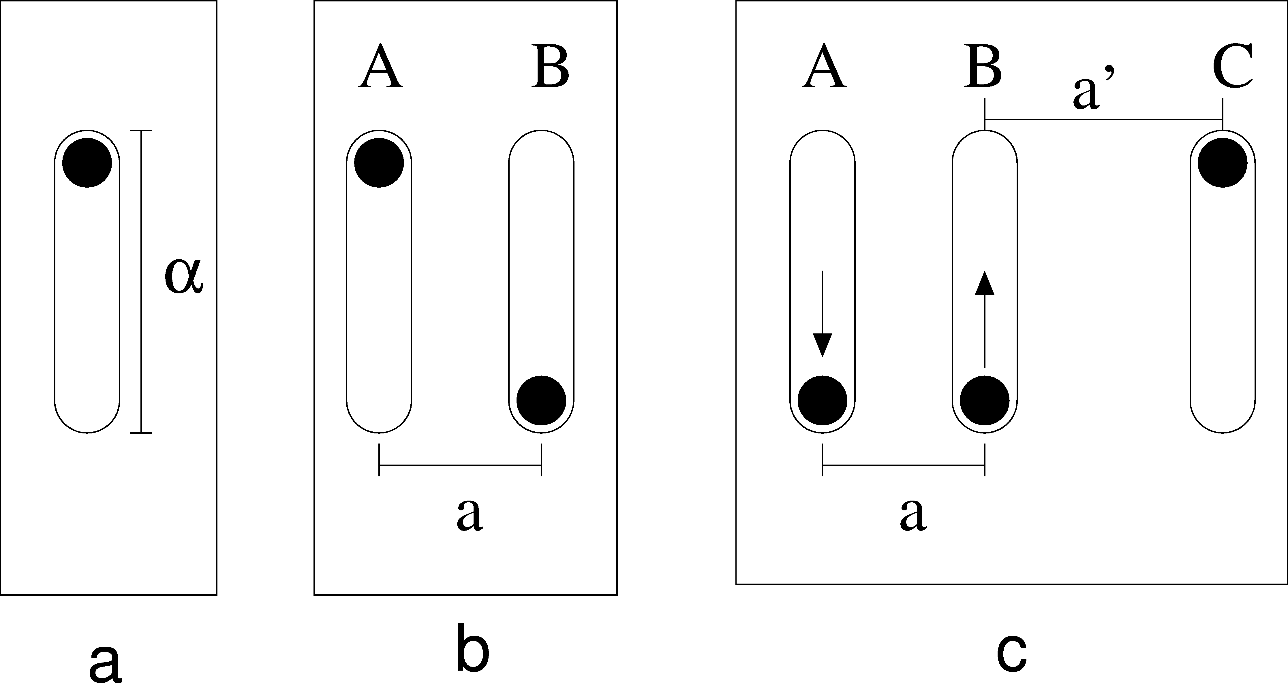
Figure 1:
(a) A single antidot of elongation α, containing a vortex indicated by
the filled circle. (b) Vortices in two antidots separated by a distance
a move to opposite ends of the wells. (c) Addition of a third antidot
at spacing a′ > a.
In superconducting samples that have been nanofabricated with an
array of pinning sites, an individual vortex will be captured by
each pin at the matching field
[16,17,18,19,20,21,22,23,24,25,26].
Here we consider pins in the form of blind holes, so that Abrikosov
vortices can sit inside the pins at well-defined locations.
If the pinning sites are not circular, but are instead elongated
in the plane by a length α [Fig. 1(a)],
then vortices in adjacent dots will move to the top
or bottom of each pinning site, as illustrated in Fig. 1(b).
If vortex A in Fig. 1(b) is moved from the top of the pin to the bottom
by, for example, an STM tip, then vortex B will move to the top of
its pin after a transit time ttr which can
be written
ttr=
⌠ ⌡
α
δ
dy
v(y)
,
where v(y)=f·∧y/η,
the y velocity of vortex B at position y. The integration must start
from a small offset δ because if the two vortices are at
the same
y location, they exert no force on each other in the y direction and
will not move without thermal assistance. Putting in the approximation
for the thin film interaction [27],
f(r)=f0′d/r, where
f0′=Φ02/(2πμ0λ2),
Φ0 is the elementary flux quantum, μ0 is the
permeability of free space,
λ is the London penetration depth of the superconductor,
and d is the thickness of
the superconducting film,
gives
ttr
t0
=
1
2
(α2 − δ2) + a2 ln(
α
δ
) .
Here time is measured in units of t0=η/f0′,
distances are measured in units of d,
and η = Bc2Φ0/ρN.
For example, in the case of a Nb film of thickness 2000 Å with antidots
of anisotropy α = 3λ = 135 nm, spacing between the
dots of a = 3λ = 135 nm, and dot width δ = 0.24λ = 10.8 nm,
the transit time of ttr=27.2t0 corresponds to an actual time
of 1.4 ns, indicating that the maximum operating frequency for this
dot geometry is 696 MHz. Smaller or more closely spaced dots will operate
at higher frequencies.
To create a logic device, it is necessary to propagate the signal by
more than one well. Thus, we consider the addition of a third well,
spaced a distance a′ from the second well, as in Fig. 1(c).
If the dot spacings are equal, a=a′, then when the vortex
in dot A is switched, the vortex in dot B
will no longer be able to
switch to the new logic state since the presence of the vortex in
dot C creates a potential barrier at the center of dot B. Since vortex
B has no kinetic energy, it is unable to overcome this barrier without
the assistance of thermal activation. The barrier can also be lowered
by taking a′ > a.
We demonstrate the switching of the three-dot system by means of a
two-dimensional numerical simulation with open boundary conditions.
The equation of motion for a vortex i is
fi = ηvi = fivv+fip+fiT
where fiT is a Langevin force due to the temperature.
The pinning force fip is implemented using an
ordinary parabolic trap that has been split in half and elongated in
the y direction. In the central elongated portion of the pin,
there is no y-direction confining force. The pin strength is chosen
strong enough that each vortex remains confined within its pin at all
times. The vortex-vortex interaction is taken to be that of vortices
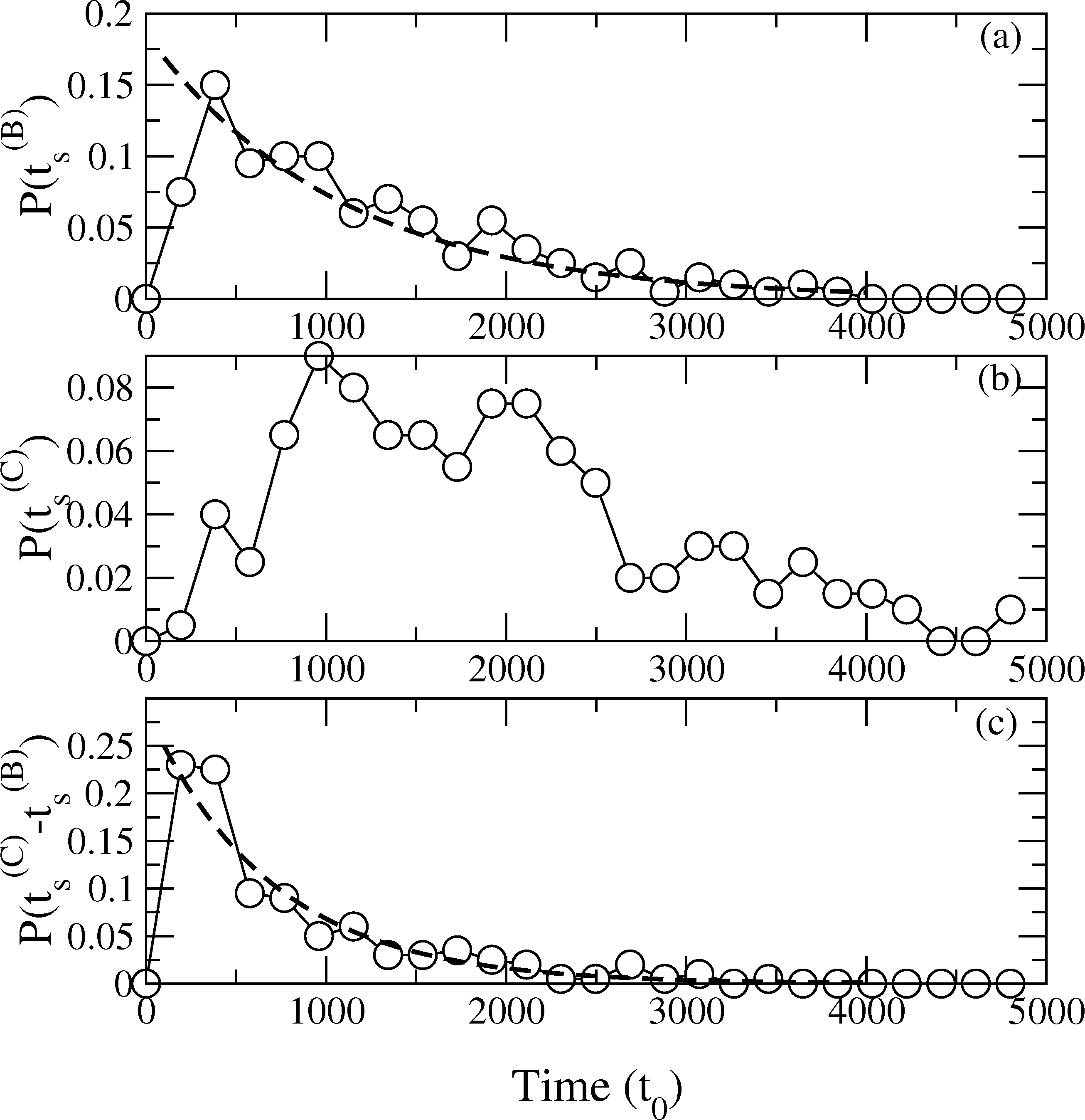
in a thin film, fvv(r)=f0′d/r. Fig. 2 shows the
distribution of switching times P(ts) for a system with
fT=1.2f0′, a=0.5λ, a′=0.68λ,
and α = 2.48, obtained from 200 runs with different random temperature
seeds. The dotted line in Fig. 2(a) indicates that the
switching time of vortex B, P(ts(B)), is exponentially
distributed, which is consistent with the thermally activated nature
of the switching. The distribution of switching times for
the third vortex C, P(ts(C)), plotted in Fig. 2(b), is
clearly broader and more heavily weighted toward later times.
P(ts(C)) is simply the product of two exponential distributions,
as can be seen from the plot in Fig. 2(c), where the distribution of
switching time for vortex C measured from the time when vortex B
switched, P(ts(C)−ts(B)), is also exponentially distributed.
Figure 2:
(a) Distribution of switching times P(ts(B)) for vortex B.
(b) P(ts(C)) for vortex C, with time measured from t=0.
(c) P(ts(C)−ts(B)) for vortex C, with time measured
from t=ts(B) for each run, the time at which vortex
B switched.
If additional wells are added, the spacing between wells n and n+1
must always exceed the spacing between wells n and n−1. This places
a practical limitation on the total length of a device that could be
constructed, since the vortices will thermally decouple once the well
spacing becomes too large. In addition, the distribution of switching
times for the final well will become increasingly broad and approach
a Gaussian as the number of wells is increased. Thus strict clocking
of the signal cannot be achieved with this approach.
The limitations listed above can be overcome by allowing the well shapes
to vary, and by introducing a ratchet mechanism which operates by altering the
spacing between neighboring vortices without requiring the wells to be
placed ever further apart as the number of wells is increased [15].
A well geometry which can be used for clocked logic operations is
illustrated in Fig. 3. The pattern consists of a series of three
alternating wells, A, B, and C. Well A is identical to the wells considered
in the first portion of this paper: it is narrow, and does not allow
significant vortex motion in the x direction. Wells B and C are both
wider,
but are biased in opposite directions. A vortex in well B will preferentially
move to the left side of the well, whereas a vortex in well B will
preferentially move to the right side of the well. The potential
required to achieve this effect is illustrated as U(x) in Fig. 3.
With this well geometry, the spacing between the vortices is not
constant. As shown in Fig. 3(a), in the absence of any driving currents,
the vortices in wells A and B are closer together (a spacing of "a"),
while the vortices in wells B and C are further apart
(a spacing of "a′"). The vortices in wells C and A are also
close together (spacing a). As a result, if the vortex in well A is
switched, as illustrated in Fig. 3(a), the vortex in well B will be able
to flip to the new state without being trapped by a potential barrier
at the center of the well, as described above for equally shaped wells
with varying spacing. The addition of a suitable potential U(y) ∝ y2
can remove this barrier completely and allow the vortex to switch without
thermal activation.
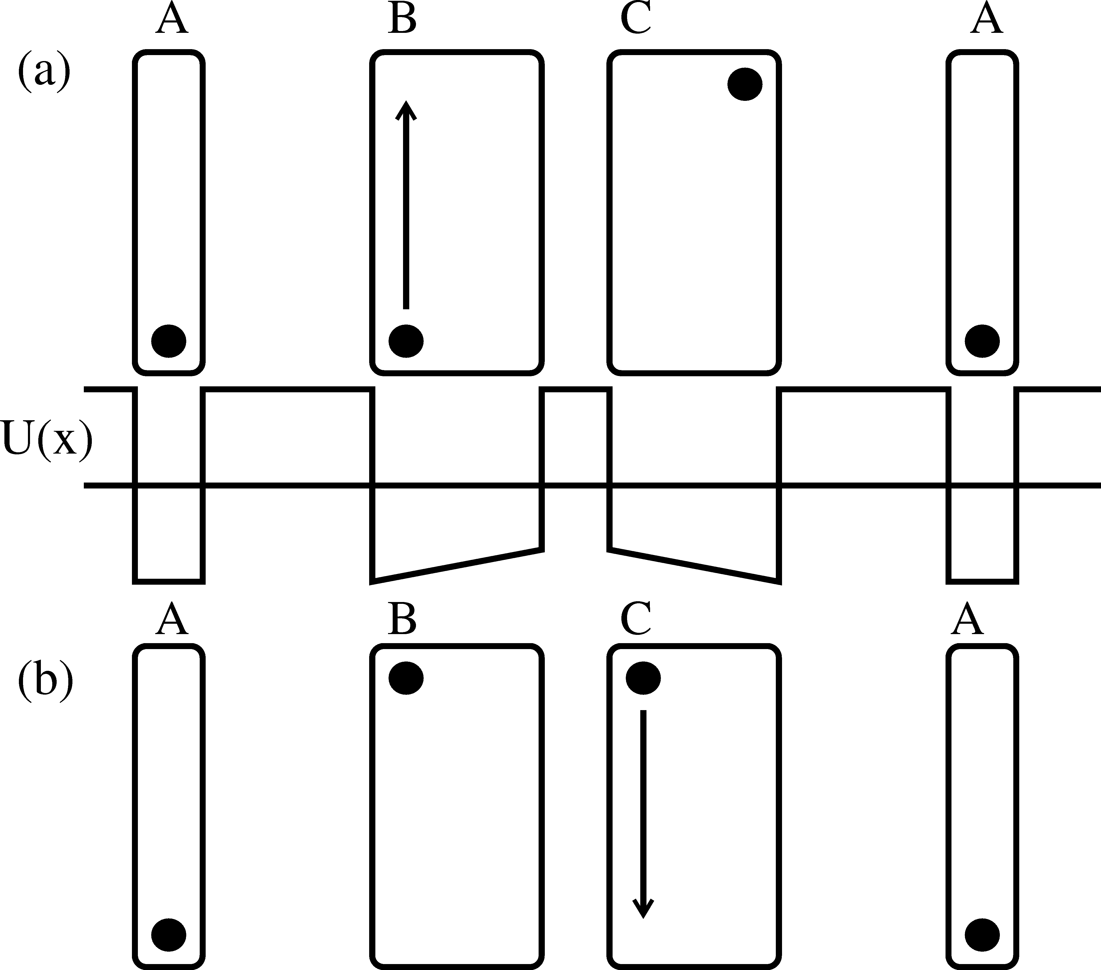
Figure 3:
(a) Schematic of well geometries used in combination with a three-stage
ac current to generate a ratchet effect. U(x) indicates the potential
of the wells as a function of x. The vortex positions and motions at
J=0 are shown. (b) Schematic of the vortex positions and motions
during the second stage of the ratchet, for J=−J∧y.
Once the signal has moved over by one well from A to B, it stops. In order
to propagate it further, we must adjust the spacing between the vortices.
We achieve this by applying a three-stage ac external current J(t).
The order of the
three stages is J=0, J=−J∧y,
and J=+J∧y. Here J is chosen large enough to
overcome the bias of wells B and C and shift the vortex to the opposite
side of the well, but not large enough to depin the vortices.
At J=0, the spacing between the vortices in wells B and C
is the far spacing a′. When we apply J=−J∧y,
as shown in Fig. 3(b),
the vortex in well C is shifted from the right side of the well to the
left side. As a result, vortices B and C are spaced by a distance
a, while vortices C and A are spaced by the larger distance a′.
Thus, vortex C is now able to flip to the new logic state. In the
third stage of the ratchet, J=+J∧y, the vortices in wells
B and C shift to the right side of the wells, so that the far spacing
a′ is now between the vortex in the rightmost well A and the
vortex in well B to the right of this well, not illustrated in the figure.
At the same time vortices C and A are now at the close spacing a,
coupling them, and allowing the vortex in the rightmost well A to flip
to the new state. As the cycle repeats, the signal continues to
propagate to the right.
The signal is prevented from moving backward due to the fact that
there are three stages of the ac drive and three shapes of
the well. This breaks the left-right symmetry of the system.
For example, in Fig. 3(b), only the vortex in well C can flip. The
vortex in well B is not able to flip back to its previous state
due to the presence of vortex A at a close spacing a from vortex B,
which inhibits the flip. The signal follows the location of the
far spacing a′ as this spacing is propagated through the
system.
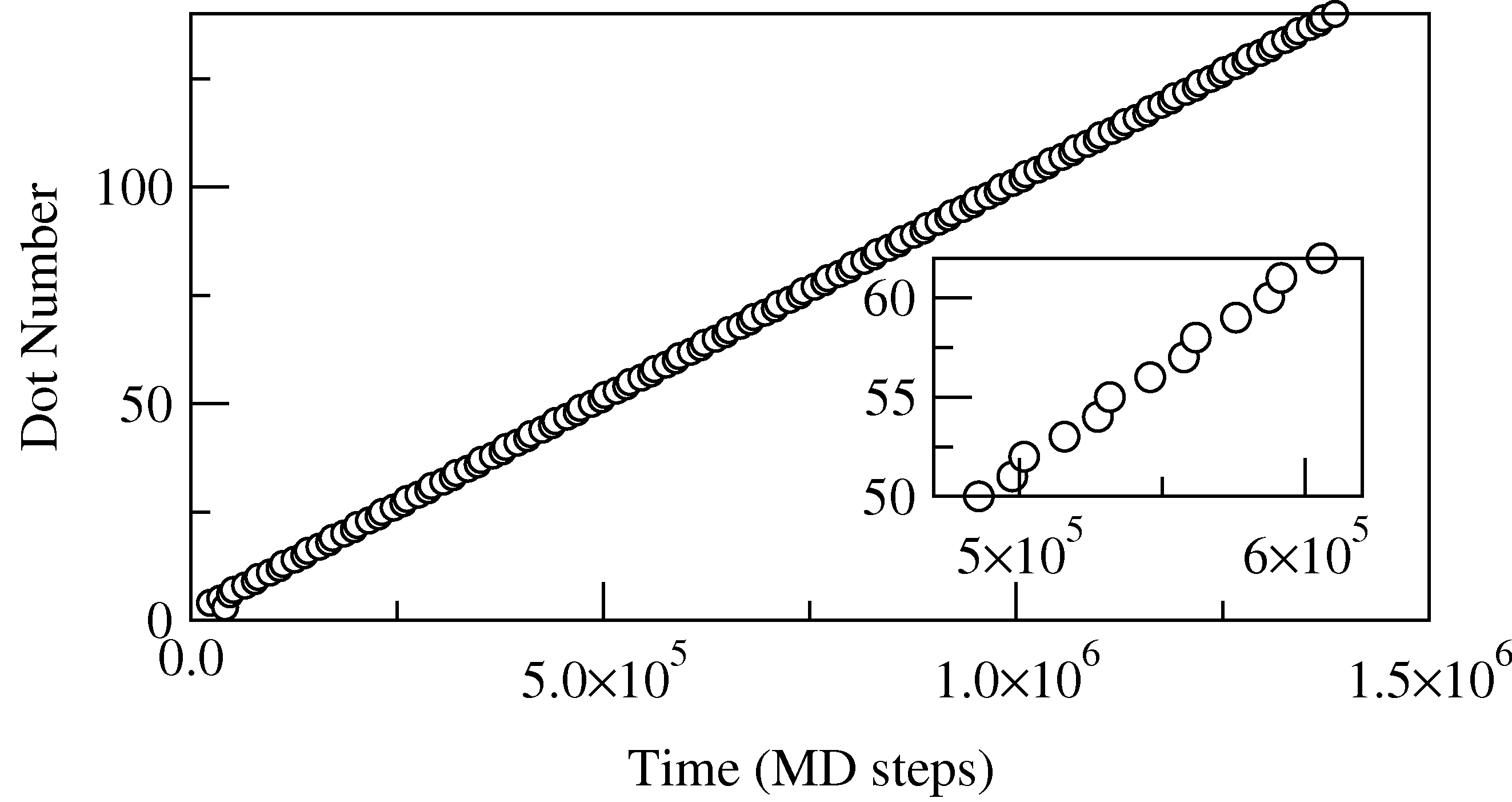
Figure 4:
Simulated signal propagation through a pipeline. The time at which
the vortex in each well changes states is indicated. Inset: Detail
showing the slight asymmetry in the switching times of the three
wells.
Figure 5:
(a) Schematic of a fanout geometry. Double arrows indicate places
where the spacing between the wells has been increased slightly in
order to achieve the desired coupling.
(b) Schematic of a NAND gate.
To illustrate that fully clocked signal propagation is possible
using the well geometry described above, we perform a simulation
of a logic pipeline composed of 144 wells with shapes A, B, and C.
The length of the repeat pattern (3 wells) is 5λ,
the
diameter of the thin well A is 0.48λ, and the diameter
of the wide wells B and C is 1λ. The close spacing
a=1.5λ while the far spacing a′=2λ. This
does not represent an optimal ratio of a/a′, which is
equal to 2, but instead was chosen to include a realistic finite
separation between the dots. The length of the wells in the
transverse direction, not counting the confining ends, is
1.2λ.
Each well also includes an additional confining
potential
U(y) ∝ y2 which removes the remaining barrier to
vortex motion.
As shown in Fig. 4, a signal introduced at one end of the pipeline
propagates perfectly through the wells, and required 10000 molecular
dynamics steps to move over by three wells. In YBCO, with
λ = 156 nm, this would correspond to a frequency
of ν = 160.2MHz. Higher frequencies can be obtained by
decreasing the sizes of the wells, or equivalently by using a
material with smaller λ. The ratchet is robust against
thermal fluctuations, and strict clocking can be
maintained if the energy scales of the ratchet potential exceeds
the thermal energy scale. An example of thermal activation combined
with the ratchet effect is given in Ref. [15].
The dissipation of the device arising from the motion of the vortices
during each stage of the ac drive is negligible, of order
10−17J. This is orders of magnitude smaller than comparable
dissipation in CMOS structures. These small dissipation energies
are similar to those for magnetic QCA devices [9].
The direction of the signal propagation can be reversed simply by
reversing the stages of the
ac drive. Additionally, it is
possible to reverse the signal propagation for the same ac drive
used above by altering the well shapes slightly. If well A is
replaced with a wider well that has a V-shaped U(x), such that
the vortex sits at the center of the well for J=0 and
shifts to either side of the well during the other two segments of
the ac cycle, then the far spacing a′ will propagate
to the left instead of to the right. This would allow two pipelines
operating in opposite directions to be driven by the same clocking
current.
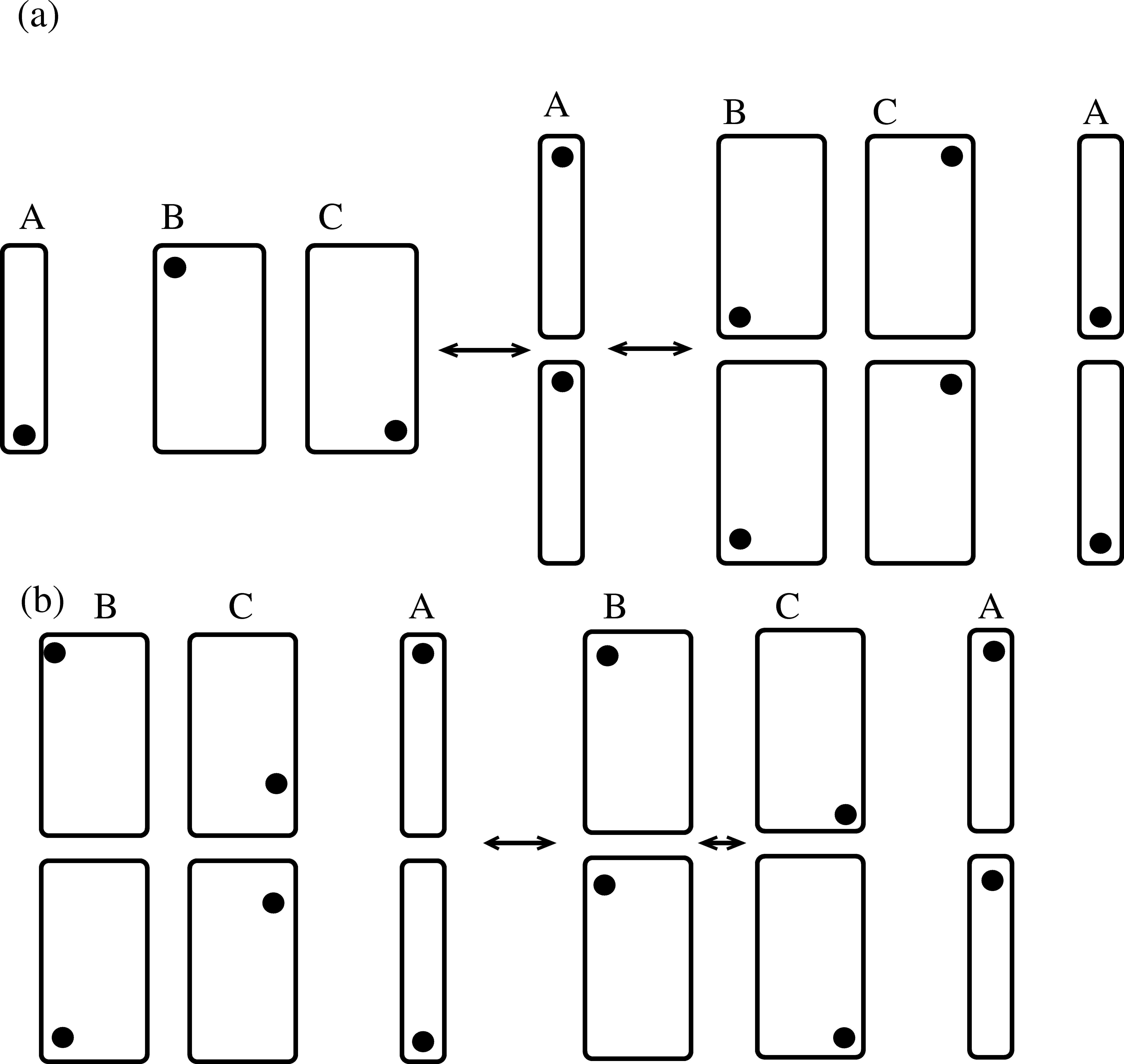
Figure 6:
XOR gate using wire-crossing.
Logic gates can be created from the ratchet geometry by coupling
more than one pipeline together vertically, and introducing specific
modulations in the well spacing to control the
coupling. For
example, a fanout, which splits one logic
pipeline into two, is illustrated
in Fig. 5(a). The well spacing at the beginning of the fanout is
increased slightly in order to enable the vortex in well C immediately
to the left of the fanout to respond to its left neighbor in well B
rather than to its two right neighbors in wells A. A NAND gate is
illustrated in Fig. 5(b). There is a similar increased spacing between
wells at the point where the two pipelines couple to produce a single
signal. A slight upward bias is applied to the vortices in the
center A and B cells (which serve as the gating cells), in order to
give the system a preferred state if the inputs are in an opposite state,
thus producing the NAND logic [28].
Very complex designs for gate arrays
can be constructed using a large number of neighboring pipelines
with spacing that is varied in selected places.
The basic ratchet naturally functions as an inverter. The gate
shown in Fig. 5(b) can be used as a NAND or NOR gate, or, with an additional
inverter, an AND or OR gate. Given these gates, a full logic family
is available, and an XOR gate can be constructed from the NOT
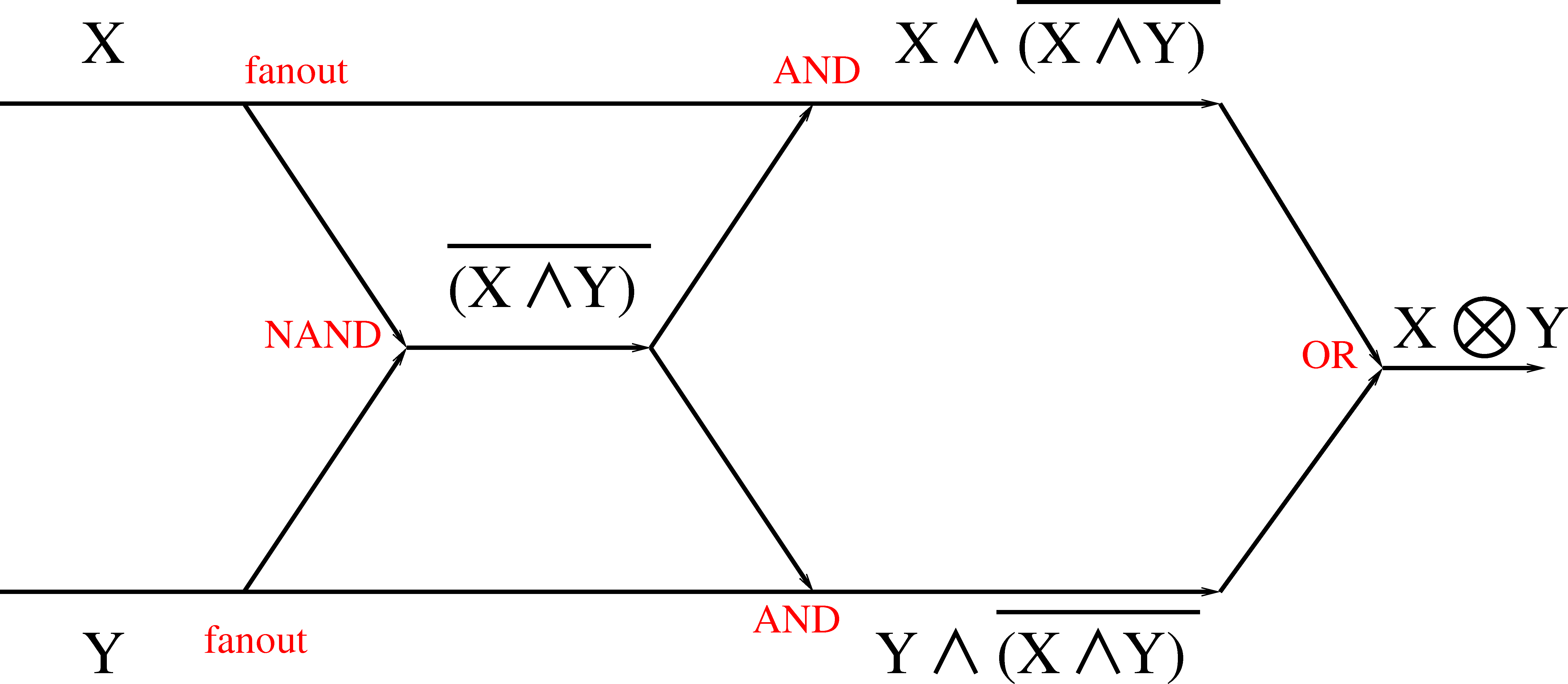
and AND gates. For example, to construct an XOR gate, one might try
X ⊗Y = (X ∨Y)∧―(X ∧Y). However, this
series of logic operations requires a wire-crossing, as shown in
Fig. 6.
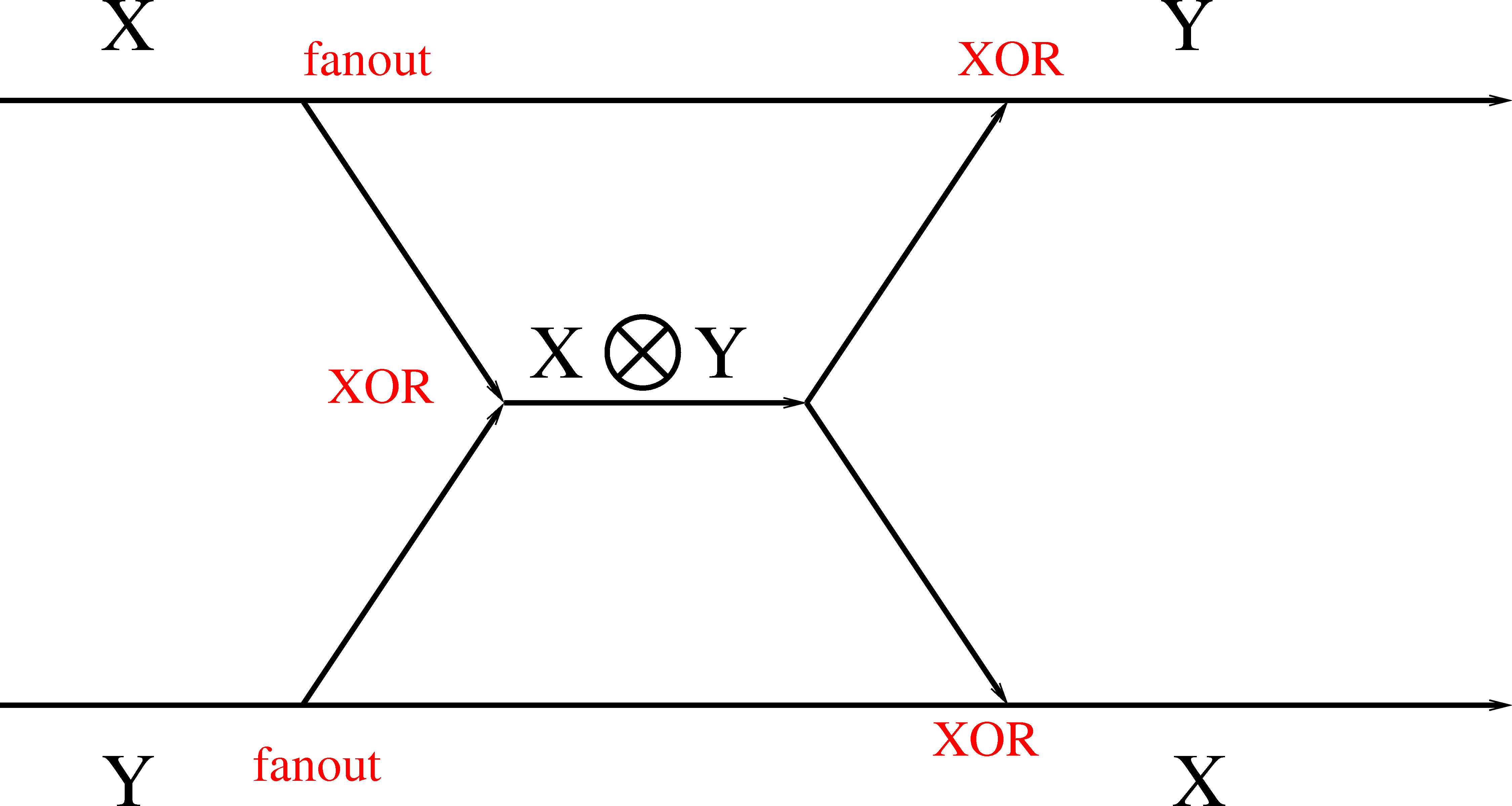
While it may
be possible to implement a wire-crossing with a bi-layer material, there is
an alternate means of constructing the XOR gate without crossing
any wires. This is shown in Fig. 7. We use
X⊗Y = (X∧―(X ∧Y))∨(Y∧―(X ∧Y)).
From this XOR gate, one
can construct a series of gates that functions as
a wire-crossing, as shown in Fig. 8, where we use
Y=X⊗(X⊗Y) and
X=Y⊗(X⊗Y).
Figure 7:
XOR gate without wire-crossing.
The ratchet effect illustrated here for a superconducting vortex
system can be generalized to other systems in which the position of
individual particles is used to represent logic states.
For example, for electron charges in a quantum dot, such as in the
QCA architecture, the maximum operating frequency would be set by
the level spacing of the dot, and would be higher than the frequencies
achieved here. Faster operating speeds can also be obtained by
using Josephson vortices, which have no normal core.
Our system may also be realizable for ions in dissipative optical light
arrays with damped ion motion where the potentials can be tailored
by adjusting the optical landscape [29]. In addition,
a variation of this system could be constructed using charged
colloidal particles in optical trap arrays [30],
where the colloids can be driven with an electric field, an ac fluid
flow, or by oscillating the trap.
Figure 8:
Wire crossing constructed from XOR gates.
In summary, we have proposed a ratchet mechanism to produce clocked
logic operations for discrete particles such as vortices in
nanostructured superconductors by using an applied ac drive combined
with three repeating trap shapes. We have shown using numerical
simulations that this ratchet effect can overcome the limitations of
using equally shaped wells operated by thermal activation, where
clocking could not be achieved. Our results should be generalizable
for other systems such as single electrons in quantum dots,
Josephson vortices, and ions in optical traps.
We thank
W. Kwok and T.A. Witten for useful discussions.
This work was supported by the US DoE, Office of Science, under Contract
No. W-31-109-ENG-38.
CJOR, CR, and MH were supported by the US Department of Energy under Contract
No. W-7405-ENG-36. BJ was supported by NSF-NIRT award DMR02-10519 and the
Alfred P. Sloan Foundation.
B. Cheng, M. Cao, R. Rao, A. Inani, P.V. Voorde,
W.M. Greene, J.M.C. Stork, Z. Yu, P.M. Zeitzoff, and J.C.S. Woo,
IEEE Trans. Elect. Dev. 46 (1999) 1537.