Physical Review Letters 90, 247004 (2003)

Ratchet Cellular Automata

M. B. Hastings1, C. J. Olson Reichhardt2, and C. Reichhardt1

1Center for Nonlinear Studies and 2T-12, Theoretical Division, Los Alamos National Laboratory, Los Alamos, New Mexico 87545

(Received 14 November 2002; published 19 June 2003)

In this work we propose a ratchet effect which provides a general means of performing clocked logic operations on discrete particles, such as single electrons or vortices. The states are propagated through the device by the use of an applied AC drive. We numerically demonstrate that a complete logic architecture is realizable using this ratchet. We consider specific nanostructured superconducting geometries using superconducting materials under an applied magnetic field, with the positions of the individual vortices in samples acting as the logic states. These devices can be used as the building blocks for an alternative microelectronic architecture.
As the size scale for microelectronics continues to decrease, limits to the efficiency of standard architectures will at some point be exhausted which will mandate the necessity of switching to alternative device architectures[1]. Any such architecture requires a means of storing state information, as well as a means of performing logic operations in a clocked fashion on the state information.
In this work, we propose a means of performing logic operations based on a novel deterministic ratchet mechanism. This provides a general means of computing with discrete particles, be they vortices in superconductors, single electrons in coupled quantum dots, Josephson vortices, or ions, via a non-equilibrium drive applied to the system.
The use of single electron charges for storing state information has been well studied. An example of this is the quantum dot cellular automata (QCA)[2,3] where the positions of the electrons are used to create the logic states and adiabatic changes are performed to the system Hamiltonian, so that logic operations are performed with the system always remaining in its ground state. A magnetic version of the QCA has also been proposed [4]. One disadvantage of QCA is that it is currently limited to operation at very low temperatures. Further, the need to perform adiabatic changes to the Hamiltonian limits the processing speed. The ratchet mechanism discussed in this paper provides a means of significantly increasing this speed.
A different approach to storing information is to use superconducting nanostructured arrays in a magnetic field where positions of the vortices define the logic state[5]. This is the specific system we consider in this paper to numerically demonstrate the feasibility of our ratchet. When a magnetic field is applied to a superconductor, the flux enters in the form of individual quantized vortices which repel each other and form a triangular lattice. Recent work on mesoscale superconductors has demonstrated that individual vortices can be captured in a single sample [6,7,8]. Additionally, several groups have nanostructured the surface of a superconductor with pinning sites which act as areas that capture vortices [9,10,11]. These nanostructured arrays are made by creating magnetic or non-magnetic dots, and the dot geometry of the individual dots can be controlled. Consider two parallel elongated dots or pinning sites with the elongation in plane and a magnetic field perpendicular to the plane at a strength such that each dot captures exactly one vortex. If the dots are in close proximity, then the positions of the vortices in the two dots will be correlated due to their mutual repulsion. The vortices will be arranged such that one vortex is located at the top of the dot and the other at the bottom of the adjacent dot. The state with the vortex at the top we consider to be a logic value of 1, while the state where the vortex is at the bottom of the dot is a logic 0. Experiments and simulations on small 2×2 superconducting arrays have observed such states[5,12].
In order to create logic devices based on these dots, we require a mechanism for propagating a flip or change of logic state through the dot array, as well as to perform logic operations. Further, the new state must propagate at a constant rate so that a constant clock speed can be achieved. For the simplest geometry of Fig. 1(a), alternate vortices prefer to align in opposite logic states due to repulsion between the vortices. We have indicated a defect at the left of this configuration, and ideally would like this defect to propagate to the right by flipping vortices, carrying new state information. However, since the vortex system is dissipative, moving the defect requires thermal activation and is hence slow and equally likely to occur in either direction. To remedy this, we propose a means of propagating information entirely distinct from that in the QCA system: in a suitable dot geometry, deterministic mechanical ratchet effects can be used to drive the system from one state to the next[14]. Our defect ratchet mechanism propagates defects in a fixed direction along the chain, in contrast to other soliton ratchets which propagate different defects in opposite directions [15]. The dissipative nature of the dynamics increases the speed of the device, while the short distance traveled by the vortices in the device limits the power consumption to very low levels.
fig1.png
Figure 1: (a) Pipeline without ratchet. (b) Schematic of ratchet for pipeline. U(x) indicates potential as a function of x. Positions and motion of vortices are indicated at J=0. (c) Schematic of second stage of ratchet, for J=−Jy.
To describe the ratchet, we recall that a vortex is well modeled as an overdamped particle so that the velocity v is proportional to the net force on it, where the force arises from vortex-vortex interaction, the confining potential which is produced by varying the film thickness, and Lorentz forces due to any applied external current. The equation of motion is then
F = η v = Fvv + Fs + Fac
(1)
where η is the viscous damping coefficient and Fvv is the repulsive vortex-vortex interaction. The force from the confining potential is Fs = − ∇U(x,y)r, and Fac is the Lorentz force from an applied ac current J, Fac = J(t)×hΦ0d, where Φ0 = 2.07×10⁻¹⁵ T m2 is the elementary flux quantum of one vortex and d is the sample thickness. The applied H is out of the plane in Fig. 1. To drive the ratchet, we apply a current, uniform across the sample, in the y-direction, producing a Lorentz force that moves the vortices in the x-direction. To obtain a uniform current, it may be necessary to attach multiple leads to the sample to deal with sample inhomogeneities. Additional current in the x direction can be applied locally to change the state of individual vortices and to enable input to the vortex logic. Readout from the logic can be handled using an STM or the recently demonstrated "vortex quantum switch" [16], and can be improved by adding elongated "readout cells" which produce a larger change in the magnetic field for a change in logic state.
In Fig. 1(b) we show the basic ratchet mechanism to propagate logic information along a pipeline. There are three different types of potential wells, labeled by letters A, B, and C and alternating in that pattern. The A wells are narrow, so that vortices in these wells have little ability to move in the x-direction. The B and C wells are both wider, with the B well having an overall tilt in the potential to the left side of the well and the C well having a tilt to the right side. The form of U(x) is illustrated below Fig. 1(b), where we plot U(x) along a line passing through the center of the wells. To drive the ratchet, the external field J(t) is driven through a series of states, J=0, J=−J y, and J=+Jy, consecutively. The external current is taken sufficiently strong so that for JJy it can push the vortex to the left or right side, respectively, of the well, overcoming the tilt in U(x) in the B and C wells, while at J=0, the tilt in the B and C wells determines the x-position of the vortices. Thus, the spacing between the vortices changes as J changes, with a narrow spacing between some and a wide spacing between others, altering the strength of the interaction between different neighbors. The lowest energy state for the system is to put the defect between vortices which have the furthest spacing. For J=0, this is between wells B and C; for J=−Jy it is between wells C and A; and for J=+J y it is between wells A and B. Thus, if the left-most vortex is held fixed in Fig. 1(b), at J=0, the vortex in the B well moves upward as indicated by the arrow. Then J is switched to −Jy and the vortices move as indicated in Fig. 1(c). Finally, switching J to +Jy moves the defect one more position to the right, and the ratchet can repeat. In this process, the alternating current raises the energy of the system by moving the vortices; this energy is then dissipated as the vortex moves. However, there is still an energy barrier to the vortex motion. As the vortex in the B well moves upward in Fig. 1(b), its energy initially increases, before dropping as the vortex completes its motion. By adding a suitable additional potential U(y) ∝ y2, we are able to remove this barrier, changing the thermal ratchet into a deterministic ratchet.
We demonstrate numerically the operation of these devices via simulation. The optimal geometry of the dots has the ratio between the wide and narrow horizontal spacings between vortices equal to 2. To include a realistic finite separation between dots, we considered ratios of 1.3−1.5. Larger ratios increase the speed of the device and enable the device to work over a wider range of potentials U(x,y). The range of allowed potentials is such that devices can be built which are robust against small fluctuations in the experimental geometry. We consider two types of vortex-vortex interactions. The first, appropriate for bulk samples, is Fvv = (Φ02 d/2πμ0λ3) K1(r/λ)r, where K1(r/λ) is the modified Bessel function that falls off monotonically with r, and λ is the London penetration depth. The second form we consider, appropriate for a thin film superconductor, is Fvv = (Φ020 πΛ)r/r, where Λ is the thin film screening length[17].
fig2.png
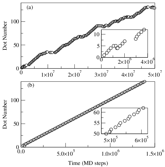
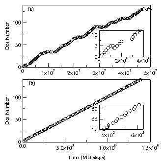
Figure 2: Simulated signal propagation through a pipeline. The time at which the vortex in each well changes states is indicated. (a) Thermally activated ratchet operating at T=0.5. Inset: Detail of the occasional backward and nonpropagating motion of the signal. (b) Deterministic, perfectly clocked ratchet at T=0. Inset: Detail showing the slight asymmetry in switching times of the three wells.
In Fig. 2(b) we show the results from a simulation of a pipe line, with a geometry where the flip propagates linearly in time with the AC drive. Fig. 2(a) shows the thermal ratchet for the case without the additional potential U(y) ∝ y2, indicating occasional reverse steps. In these simulations we considered a pattern of 144 wells with a repeat pattern length of 5λ, thin well diameter 0.48λ, and wide well diameter 1λ. The close spacing was 1.5λ and the far spacing was 2λ. The length of the wells in the transverse direction, not counting the confining ends, was 1.2λ. The simulation illustrated in Fig. 2(b) required 10000 molecular dynamics steps to move the signal over by three wells.
In terms of real material parameters[18,19], the operating frequency can be written as ν = 3/(dt τ), with the simulation time unit τ = μ0 λ3 d/(ξ2 ρN), where μ0 is the permeability of free space, d is the film thickness, which we assume to be d=200 nm, and the London penetration depth λ for selected materials is: YBa2Cu3O7−δ (YBCO), λ = 156 nm; Bi2Sr2CaCu2O8 (BSCCO), λ = 250 nm; MgB2, λ = 85 to 203 nm. The resulting frequencies are: YBa2Cu3O7−δ, ν = 160.2 MHz; Bi2Sr2CaCu2O8, ν = 86.7 MHz; MgB2, using midpoint values: ν = 315 MHz.
The frequencies above are for non-optimized well geometries, chosen instead to be readily manufactured using present day technology. Particularly in BSCCO, the average spacing between wells is 0.5μm; much smaller structures than this could be created, which would have higher operating speeds due to the larger vortex-vortex interaction forces. The maximum operating frequency of the vortex cellular automaton is set by the depairing frequency of the Cooper pair in the BCS materials. In Nb, which has a gap of ∆ = 1.55 meV, the depairing frequency is 688 GHz. YBCO, with a gap of ∆ = 20 meV, and BSCCO, with a gap of ∆ = 38 meV, have depairing frequencies in the terahertz range. Measured gaps for MgB2 range from ∆=1.8 to 7.5 meV. We can ignore the skin effect, as for the penetration depth in these materials the skin effect is irrelevant for frequencies below  ∼ 10 THz.
The dissipation of the device due to motion of the vortices is negligible: the energy to switch a single cell is of order 10−17 J for MgB2. There is an additional surface power dissipation [20], which is also small, of order 10−15 J per cycle or less. These small dissipation energies are similar to those for magnetic QCA devices [4].
fig3.png
Figure 3: (a) Schematic of fanout. The spacing between wells is slightly increased where marked by the double arrow. (b) Schematic of NAND gate. Spacing between wells is slightly increased where marked by the double arrow, to force both pipelines into the same state.
To realize a pipeline which propagates signals in reverse, the A well in Fig. 1(b) can be replaced with a wider well centered on the same point, with a potential such that the vortex is in the center of the well for J=0, and moved to the sides of the well for J ≠ 0. In order to make a complete logic architecture the basic units also include a fanout and a NAND gate, which are illustrated in Figs. 3(a-b). The exit from the fanout consists of two pipelines. Due to repulsion between particles in the neighboring pipeline, an additional potential which biases the vortices toward the bottom of the wells is added to the wells in the top pipeline, and conversely for the wells in the bottom pipeline. The well spacing at the fanout itself is slightly increased to enable the C cell immediately to the left of the fan to respond to its left neighbor rather than its two right neighbors. The spacing between the next A and B wells is also slightly increased. In the NAND gate, the pipelines before the gate have a narrower horizontal spacing. This increases the coupling between successive cells within a given pipeline, compared to that between pipelines, enabling distinct signals to propagate in each pipeline. At and after the gate, the horizontal spacing is increased, so that both pipelines must be in the same state. A slight upward bias is applied to the vortices in the gating cells (the center A and B cells) as shown, to give the system a preferred state if the inputs are in an opposite state, realizing a NAND gate. By taking a large number of neighboring pipelines and varying the spacing in selected places, a very compact design for a gate array can be constructed. The basic ratchet automatically includes an inverter, since neighboring vortices assume opposite logic states. An XOR and wire crossing can be realized using the above devices as basic components. We have also performed simulations confirming the device geometries illustrated in Fig. 3[21].
While we propose this ratchet effect in the context of information storage using vortex position, the ratchet effect can be generalized to other systems, including the case of electron charges in a quantum dot, where the maximum operating frequency will be set by the level spacing of the dot. Faster operating speeds can also be obtained using Josephson vortices. In the ratchet described above, the vortices move along the borders of the cells. By placing a thin strip of insulating material around these borders, the vortex core will exist only in the insulating material. Since there is no normal core, the dissipation η is greatly reduced and the speed increased, while retaining the very low dissipation discussed above. Our system may also be physically realizable for ions in dissipative optical light arrays with damped ion motion where the potentials can be tailored by adjusting the optical landscape [22]. A variation of this system could also be constructed using charged colloidal particles in optical trap arrays [23], where the colloids can be driven with an AC fluid flow, electric field, or by oscillating the trap.
In summary, we have shown that in order to perform clocked computations on a classical system, it is necessary to drive the system out of equilibrium. Ratchets are a fundamental aspect of non-equilibrium statistical physics that have been much studied in recent years. We have proposed a practical application of a ratchet mechanism to produce clocked logic operations for discrete particles by using an applied AC drive. With numerical simulations we have shown that a complete logic architecture can be realized. We have specifically demonstrated this mechanism for vortices in superconducting geometries. Our results should be generalizable for other systems such as single electrons in quantum dots, Josephson vortices, and ions in optical traps.
Acknowledgments- We thank B. Jánko for initial inspiration for this work, and W. Kwok and T. A. Witten for useful discussions. This work was supported by the US DOE under Contract No. W-7405-ENG-36.

References

[1]
M. Schulz, Nature 399, 729 (1999).
[2]
C.S. Lent et al., Nanotechnology 4, 49 (1993).
[3]
I. Amlani et al., Science 284, 289 (1999).
[4]
R.P. Cowburn and M.E. Welland, Science 287, 1466 (2000).
[5]
T. Puig et al., Appl. Phys. Lett. 70, 3155 (1997).
[6]
A.K. Geim et al., Phys. Rev. Lett. 85, 1528 (2000).
[7]
V.A. Schweigert, F.M. Peeters, and P. Singha Deo, Phys. Rev. Lett. 81, 2783 (1998).
[8]
C. Reichhardt and N. Grønbech-Jensen, Phys. Rev. Lett. 85, 2372 (2000).
[9]
M. Baert et al., Phys. Rev. Lett. 74, 3269 (1995); L. Van Look et al., Phys. Rev. B 60, R6998 (1999); V. Metlushko et al., Phys. Rev. B 60, R12 585 (1999).
[10]
K. Harada et al., Science 274, 1167 (1996); S.B. Field et al., Phys. Rev. Lett. 88, 067003 (2002).
[11]
J.I. Martín et al., Phys. Rev. Lett. 79, 1929 (1997); D.J. Morgan and J.B. Ketterson, Phys. Rev. Lett. 80, 3614 (1998); J.I. Martín et al., Phys. Rev. Lett. 83, 1022 (1999).
[12]
C. J. Olson Reichhardt, C. Reichhardt, and B. Jánko, unpublished.
[13]
P. Reimann, Phys. Rep. 361, 57 (2002); R.D. Astumian and P. Hanggi, Physics Today, 55, 33 (2002).
[14]
C.-S. Lee, B. Janko, I. Derenyi, and A.-L. Barabasi, Nature 400, 337 (1999).
[15]
F. Marchesoni, Phys. Rev. Lett. 77, 2364 (1996).
[16]
A. S. Mel'nikov and V. M. Vinokur, Nature 415, 60 (2002).
[17]
J. Clem, Phys. Rev. B 43, 7837 (1991).
[18]
C.P. Poole, Handbook of Superconductivity (Academic Press, San Diego, 2000).
[19]
C. Buzea, Supercond. Sci. Tech. 14, R115 (2001).
[20]
M.W. Coffey and J.R. Clem, Phys. Rev. Lett. 67, 386 (1991).
[21]
Movies of some of these simulations are available online at http://www.t12.lanl.gov/home/olson/VCA.html.
[22]
M.T. DePue C. McCormick, S. Lukman Winoto, S. Oliver, and D.S. Weiss, Phys. Rev. Lett. 82, 2262 (1999).
[23]
M. Brunner and C. Bechinger, Phys. Rev. Lett. 88, 248302 (2002).


File translated from TEX by TTHgold, version 4.00.

Back to Home