Physical Review B 68, 033101 (2003)

Effect of field-effect transistor geometry on charge ordering of transition metal oxides

C.J. Olson Reichhardt, C. Reichhardt, D.L. Smith, and A.R. Bishop

Theoretical Division, Los Alamos National Laboratory, Los Alamos, New Mexico 87545

(Received 18 November 2002; published 1 July 2003)

We examine the effect of an FET (field-effect transistor) geometry on the charge ordering phase diagram of transition metal oxides using numerical simulations of a semiclassical model including long-range Coulomb fields, resulting in nanoscale pattern formation. We find that the phase diagram is unchanged for insulating layers thicker than approximately twice the magnetic correlation length. For very thin insulating layers, the onset of a charge "clump" phase is shifted to lower values of the strength of the magnetic dipolar interaction, and intermediate diagonal stripe and geometric phases can be suppressed. Our results suggest that, for sufficiently thick insulating layers, charge injection in an FET geometry can be used to experimentally probe the intrinsic charge ordering phases in these materials.
Charge ordering in doped transition metal oxides has attracted considerable recent interest, both in theory and experiment. Due to the competing long-range, e.g., Coulomb, repulsion and short range antiferromagnetic interactions in the charge system, a rich variety of phases can occur, including stripes [1,2], clumps [3,4], and liquid crystalline electron states [5]. Simulation studies of the charge ordering phase diagram [6,7] showed transitions among four phases depending on the hole density and the strength of a dipolar interaction induced by the holes: a Wigner crystal at low hole densities, a diagonal stripe phase, an intermediate geometric phase in which the charges form continuous filaments in a square checkerboard pattern, and a clump phase at larger dipole interaction strengths. The behavior of these phases is of interest not only for the charge ordered system, but also for their similarities to other pattern forming systems with coexisting short- and long-range interactions, including magnetic films [8], Langmuir monolayers, polymers, gels, and water-oil mixtures [9]. A natural extension of this model is to consider charges interacting with a distortable charged membrane, which could be relevant to active membrane systems such as ion pumps.
To experimentally probe the charge ordering phase diagram, the hole doping of the material must be controlled. A recently proposed method of controllably varying the hole density is the use of a field effect transistor (FET) geometry to inject holes into the metal oxide plane. The geometry is illustrated in Fig. 1. An insulating layer is deposited on top of the metal oxide, and then a metallic gate is deposited on top of the insulator, forming a capacitive structure. By varying the gate voltage, holes move into or out of the metal oxide layer, allowing the sample to be conveniently tuned to the desired doping level [10]. Source and drain contacts can be used to probe the conductance properties of the structure. A potential drawback of this geometry for exploring the phase diagram is that the holes can interact with the gate layer, and complicate the intrinsic hole-hole interactions within the metal oxide which lead to the charge ordered phases: the phases could be distorted or disrupted by the presence of the FET geometry.
To asses the effect of an FET geometry on the charge ordering phases, we simulate a model of a single metal oxide layer interacting with a metallic gate layer that is offset by varying thicknesses of insulating material. We find that for a sufficiently thick insulating layer, the charge ordering is unaffected by the presence of the gate. When the insulating layer thickness approaches twice the magnetic correlation length in the metal oxide, however, we find a sharp downward shift in the onset of the clump phase as a function of dipole interaction strength. The diagonal stripe and geometric phase boundaries do not shift, but these phases can be suppressed by the intrusion of the clump phase as the insulating layer is made thinner. Our results show that, for sufficiently thick insulating layers, the FET geometry should provide a reliable probe of the charge ordering phase behavior.
Fig1.png
Figure 1: Schematic of the FET geometry considered here. "S" and "D" represent the source and drain contacts, respectively. The vertical scale of the figure is exaggerated.
We consider a sample constructed in an FET geometry, illustrated in Fig. 1. The metal oxide plane is parallel to the insulating layer and also to the metallic gate layer deposited on top of the insulator. Experimentally, a gate voltage would be used to tune the doping level present in the metal oxide layer. We simulate this effect by directly varying the hole density in our system, which is a rectangular computational box of size Lx ×Ly, with Lx, Ly up to 100 unit cells in a CuO2 plane. At the beginning of each simulation, we place the holes at random and assign to each hole a magnetic dipole moment of constant size, but random direction. We find the minimum of the total potential in this system using the efficient Monte Carlo method described in [7].
Our model for the interactions between the charges is based on the spin density wave picture of the transition metal oxides. Full details of the model can be found in [6,7], but we summarize the essential details here. We use a numerical approach to simulate holes moving in an antiferromagnetic (AF) insulator in the presence of long-range Coulomb forces. We study a quasiclassical limit of the quantum problem of holes in an AF spin environment, using the model in Refs. [6,7], which incorporates the essential correlations for an effective hole-hole interaction. The AF background is integrated out, and the focus is on the charge subsystem. In the absence of disorder, this model produces four phases depending on the density of holes and the characteristic AF energy scales: a Wigner crystal, diagonal stripes, horizontal-vertical stripes (loops), and a clumped phase.
Our numerical approach utilizes the spin-density-wave picture of Schrieffer, Wen, and Zhang [11], which is closely related to the semiclassical approach to the model of Shraiman and Siggia [12] in which the interaction between doped holes stems from the spiral distortion of the local Néel vector near a hole. The SDW picture of layered transition metal oxides has been successful in describing the stoichiometric insulating AF phase of these systems at low temperatures [11]. In this model, an electron moves in the self-consistent staggered field of its spin. The electronic band is split into upper and lower Hubbard bands [13] separated by the Mott-Hubbard gap, ∆. At half filling the upper band is empty and the lower one is full. We consider a system at T << ∆/kB that is doped with holes with planar density σs, and focus on the lower band which has a maximum at ki = Q/2 = (±1, ±1)π/2a, where a is the lattice spacing. A mobile carrier in an antiferromagnet produces a dipolar distortion of the magnetic background as described Appendix B of Ref. [7]. Thus, at finite density, the holes interact via two different mechanisms: a uniform short-range attractive force due to AF bond breaking, and a long-range magnetic dipolar interaction. The latter term is due to the long-range spiral distortion of the AF background, which is a consequence of quasiparticles interacting with soft (Goldstone) modes of the spin system [12,14]. The magnetic dipole moment associated with each hole is due to the coherent hopping of holes between different sublattices and scales with the AF magnetic energy. The two-hole interaction Hamiltonian has a Fourier transform, for quasiparticle momenta near ki, of
H(r)=[Azσ1zσ2zAxy1+σ21σ2+)]δ(r)−Bxy
d1·d2

r2
−2 (d1 ·r)(d2 ·r)

r4

1+σ2 + σ1σ2+).
(1)
Here, ri is the coordinates of a hole in units of a, r=|r1r2| is the relative hole-hole distance, σiz(±)=cαfσαβz(±)cβ is a spin-density operator, σz(±) are Pauli matrices, and di is a unit vector in the direction of the dipole moment of the hole. In strictly two dimensions at finite T, the system is magnetically disordered, characterized by a finite magnetic correlation length ξ (see Ref. [15]), and the range of the dipolar interaction between the holes, mediated by the AF background, is also of order ξ. Thus, at finite T the magnetic dipolar interaction between the holes, mediated by the AF background, is actually short-ranged. The holes also interact via the long-range Coulomb interaction, which we take to be unscreened, as appropriate at low doping where rs=r0/a0 is very large: r0 is the mean interparticle distance, a0 is the Bohr radius, and rs ≈ 8. Each hole also carries a spin degree of freedom, but it can be shown [6,7] that the overall spin energy is minimized in the spin antisymmetric channel, as we assume here. Hence we neglect the spin-symmetric channel and only consider the charge channel with an effective (magnetic in origin) interaction between two holes, 1 and 2, a distance r apart in a single metal oxide plane, in the form
V(r)= q2

r
Aer/aBcos(2θ−ϕ1−ϕ2)er.
(2)
Here, q is the hole charge, θ is the angle between r and a fixed axis, and ϕ1,2 are the angles of the magnetic dipoles relative to the same fixed axis, which we assume can take an arbitrary value. A is the strength of the short-range anisotropic interaction, and B is the strength of the magnetic dipolar interaction [BA/(2πξ2)], which we assume to be independent variables. In real cuprate oxide materials, B should be of order  ∼ 1eV. Throughout this work we take A=0. Since the isotropic attractive interaction due to the second term in Eq. 2 is extremely short-range (in fact in an infinite system it is a δ function), it is initially reasonable to set A=0 and explore the behavior of the system as a function of B. The magnetic correlation length ξ is obtained from neutron scattering measurements [16], and here we assume the approximate dependence ξ = 3.8/√n Å. The doping level n is defined as the hole density measured in units of the cuprate lattice spacing. Thus n=1% corresponds to 1 hole per 100a2, where a ≈ 3.8Å. We have assumed for numerical convenience that r can be relaxed from a crystal lattice position to an arbitrary (continuous) value. The results presented here are for a system with 196 holes with size ranging from 307.15Å × 307.15Å  (for n=3%) to 137.4Å × 137.4Å  (for n=15%). The value of ξ then ranges from 21.9Å  for n=3% to 9.8Å  for n=15%. The sample is periodic in the x-y plane [17].
In the FET geometry, a metal oxide channel is created, then an insulating layer of thickness d is deposited on top of the channel, and finally a layer of metal is deposited to serve as a gate. The interactions between holes in the metal oxide layer is altered by the presence of image charges in the gate layer,
∇·D=4πρ = 4πe

i 
[δ(r−(r||i+d
^
z
 
)) − δ(r−(r||id
^
z
 
))] ,
(3)
giving the Coulomb energy between charges a distance d into the material as
E= e2


ij 


1

|r||jr||i|
1

|r||jr||i+2d
^
z
 
|


.
(4)
Thus, we modify the Coulomb interaction between the holes in our system to this form. This introduces a new length scale 2d. For comparison, we also ran simulations with the unmodified Coulomb interaction, representing a bare metal oxide plane without the FET gating.
Fig2.png
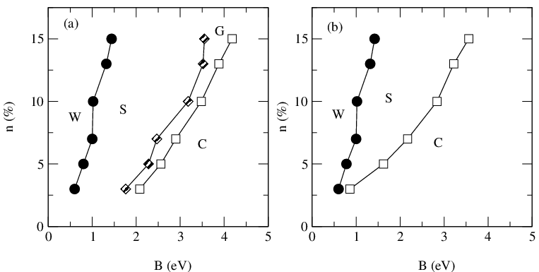
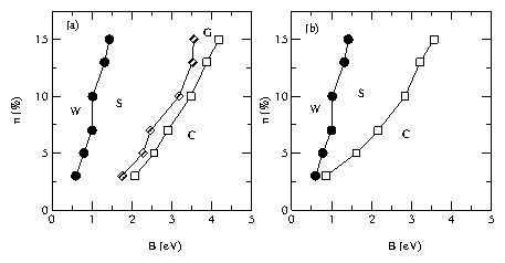
Figure 2: (a) Phase diagram as a function of the hole density n and the strength of the magnetic dipolar interaction B, for a sample without the FET interaction term, Eqn. 4. "W" is the Wigner crystal phase, "S" is the diagonal stripe phase, "G" is the geometric phase, and "C" is the clump phase. (b) Phase diagram for a sample with the same parameters but with the FET interaction added at an insulator thickness of 14Å, showing the downward shift in B of the clump phase "C," and the suppression of the geometric phase "G".
In the absence of the FET interaction, we find a phase diagram consistent with that observed in Ref. [6], as illustrated in Fig. 2(a). For thick insulating layers, when the FET interaction is included, the locations of the phases are not affected and we obtain the same phase diagram, as shown in Fig. 2(a). As we decrease the thickness of the insulating layer, however, we find a crossover thickness dc below which the phase boundaries begin to change. Fig. 2(b) illustrates the phase diagram for the same system as in Fig. 2(a) but with the FET term added and with an insulating layer of thickness d < dc (d=14 Å). The onset of the diagonal stripe phase "S" is unaffected, but there is a large shift downward to BC of the onset of the cross-like clump phase "C." The size of the downward shift, ∆B, increases as the hole density n decreases. The geometric phase that was present without the FET term is now completely suppressed.
Fig3.png
Figure 3: The clump phase at two different hole densities. (a) n=13%, ξ = 10.54Å. (b) n=3%, ξ = 21.9Å.
The interplay of the correlation length and the insulator thickness affects the onset of the clump phase because only the clump phase possesses a characteristic length scale of order 2ξ. This is illustrated in Fig. 3, which shows the clump structure at n=13% and n=3%. When the length scale of the insulating layer is comparable with the length scale of the clump structure, the interaction with the metal gate above the insulating layer becomes comparable with the interaction with neighboring clumps, and the transition to the clump phase is enhanced.
Fig4.png
Figure 4: Phase diagram as a function of the thickness of the insulating layer d and the strength of the magnetic dipolar interaction B, for a sample with the FET interaction term, Eq. 4, and with hole density n=3%. Inset: Dependence of the cutoff thickness dc on the magnetic correlation length ξ.
The effectiveness of the FET term extends only to insulator thicknesses d that are approximately twice the magnetic correlation length, d <~2ξ. This is illustrated in Fig. 4 for a sample with n=3% and varying insulator thicknesses d. The arrow indicates the saturation of the clump phase onset BC at dc to the value of B=BC0 observed in the absence of the FET term. The other phase boundaries, Wigner to stripe and stripe to geometric, shift very little with d but instead the intermediate phases are suppressed when BC moves below the onset values for these phases. To assess whether the magnetic correlation length is responsible for the shift in the phases, we considered a system at n=13%, which normally has a correlation length of ξ = 10.54 Å, and artificially changed the screening length to ξ = 20 Å  for one series of runs, and to ξ = 5 Å  for a second series. In the inset of Fig. 4, we show the cutoff insulator thickness dc beyond which the FET term has no effect as a function of correlation length ξ, both for the normal screening lengths and for our two artificially changed screening lengths. We indeed find a linear dependence for the cutoff thickness on the correlation length, viz. dc ≈ 1.7 ξ.
In conclusion, we have found that the FET geometry does not affect the clump ordering phases unless the insulating layer is thin enough, namely less than approximately twice the magnetic correlation length. For thin insulating layers the onset of the clump phase is enhanced. This suggests that the FET geometry with a sufficiently thick insulating layer is suitable for studying the effects of hole concentration on the charge ordering phases because the presence of the FET does not alter the hole-ordered structures. Alternatively, FET geometries deliberately created with thin insulating layers can be used to probe the clump phase at higher hole densities, where the underlying value of B may preclude reaching the clump state in the bulk phase.
This work was supported by the U.S. Department of Energy under Contract No. W-7405-ENG-36.

References

[1]
V.J. Emery and S.A. Kivelson, Physica C 209, 597 (1993).
[2]
V.J. Emery, S.A. Kivelson, and O.V. Zachar, Phys. Rev. B 56, 6120 (1997).
[3]
A.A. Koulakov, M.M. Fogler, and B.I. Shklovskii, Phys. Rev. Lett. 76, 499 (1996).
[4]
M.M. Fogler, A.A. Koulakov, and B.I. Shklovskii, Phys. Rev. B 54, 1853 (1996).
[5]
E. Fradkin and S.A. Kivelson, Phys. Rev. B 59, 8065 (1999).
[6]
B.P. Stojkovic, Z.G. Yu, A.R. Bishop, A.H. Castro Neto, and N. Grønbech-Jensen, Phys. Rev. Lett. 82, 4679 (1999).
[7]
B.P. Stojkovic, Z.G. Yu, A.L. Chernyshev, A.R. Bishop, A.H. Castro Neto, and N. Grønbech-Jensen, Phys. Rev. B 62, 4353 (2000).
[8]
M. Seul and R. Wolfe, Phys. Rev. A 46, 7519 (1992).
[9]
W.M. Gelbart and A. Ben Shaul, J. Phys. Chem. 100, 13169 (1996).
[10]
T. Li, J.W. Balk, P.P. Ruden, I.H. Campbell, and D.L. Smith, J. Appl. Phys. 91, 4312 (2002).
[11]
J.R. Schrieffer, X.G. Wen, and S.C. Zhang, Phys. Rev. B 39, 11663 (1989).
[12]
B.I. Shraiman and E.D. Siggia, Phys. Rev. B 40, 9162 (1989).
[13]
N.F. Mott, in Metal-Insulator Transitions (Taylor & Francis, London, 1974), p. 141.
[14]
D.M. Frenkel and W. Hanke, Phys. Rev. B 42, 6711 (1990).
[15]
S. Chakravarty, B.I. Halperin, and D.R. Nelson, Phys. Rev. Lett. 60, 1057 (1988).
[16]
R.J. Birgeneau, D.R. Gabbe, H.P. Jenssen, M.A. Kastner, P.J. Picone, T.R. Thurston, G. Shirane, Y. Endoh, M. Sato, K. Yamada, Y. Hidaka, M. Oda, Y. Enomoto, M. Suzuki, and T. Murakami, Phys. Rev. B 38, 6614 (1988).
[17]
N. Grønbech-Jensen, G. Hummer, and K.M. Beardmore, Mol. Phys. 92, 941 (1997).


File translated from TEX by TTHgold, version 4.00.

Back to Home